

_ بخش شناخت از(آی سی های میکرو BGA) یا(میکرو پایه توپی)
بررسی ساختار و ساختمان داخلی چیپ میکرو BGA (حافظه نگه دارنده یا MEMORY) از نوع میکرو BGA یا میکرو پایه توپی حافظه
پژوهشگر و نویسنده: دکتر ( افشین رشید)

نکته: آیسی MEMORY ic (پایه توپی یا میکرو BGA) حافظه ای است "فقط خواندنی" یک چیپ کوچک که بر روی بورد ها که دارای اطلاعاتی است که شرکت سازنده آن را پر میکند اطلاعات داخل این قطعه ممکن است به دفعات اجرا شود پس از اهمیت نسبتاً مهمی برخوردار است.
اطلاعات مستقر در حافظه MEMORY ic فقط خواندنی هستند و کاربران امکان پاک کردن یا حذف و تغییر اطلاعات آن را ندارند.


فرآیند ایجاد تمپلیت اولیه برای تراشه های MEMORY ic از نوع میکرو BGA یا پایه توپی دشوار است .اما مزیت حافظه MEMORY ic از نوع میکرو BGA یا پایه توپی بر برخی معایب آن غلبه می نماید. زمانیکه تمپلیت تکمیل گردید تراشه آماده شده، می تواند بصورت انبوه و با قیمت ارزان به فروش رسد.این نوع از حافظه ها از برق ناچیزی استفاده کرده ، قابل اعتماد بوده و در رابطه با اغلب دستگاه های الکترونیکی کوچک، شامل تمامی دستورالعمل های لازم به منظور کنترل دستگاه مورد نظر خواهند بود.استفاده از این نوع تراشه ها در برخی از اسباب بازیها برای نواختن موسیقی، لپ تاپ؛ تبلت ؛ هارد اکسترنال به طور انبوه انجام میگیرد.

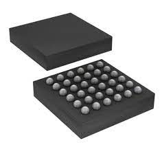
آرایه شبکه توپی میکرو «BGA » از روشی متفاوت به جای روشی که در گذشته در بیشتر اتصالات نصب سطحی رایج استفاده میشد، استفاده میکند. پکیج های دیگر نظیر بسته تخت چهار گوش یاQFP از پیرامون بسته برای اتصالات استفاده میکنند. این بدان معناست که فضای محدودی برای اینکه پینها نزدیک هم قرار بگیرند وجود دارد و برای فراهم کردن سطح مورد انتظار از اتصال ، باید بسیار کوچک باشد. آرایه شبکه توپی میکرو «BGA» از قسمت پایین بسته استفاده میکند، جایی که در آن فضای قابل توجهی برای اتصالات وجود دارد. آرایه شبکه توپی ، به دلیل نیاز به داشتن بسته قویتر و مناسبتر برای ساخت مدارهای مجتمع با تعداد زیاد پین ، بسته میکرو BGA ساخته شد.
آیسی ic حافظه تقریباً در هر دستگاه محاسباتی برای قابل اجرا و کاربردی کردن آن مورد نیاز است. حافظه MEMORY ic از نوع میکرو BGA یا پایه توپی نوعی از حافظه است، داده های ذخیره شده که در آن باقی می مانند، یعنی پس از خروج کاربر از سیستم یا راه اندازی مجدد سیستم، ناپدید نمی شوند. این به دلیل ماهیت غیر فرار حافظه MEMORY ic از نوع میکرو BGA یا پایه توپی امکان پذیر است .از آیسی حافظه MEMORY ic از نوع میکرو BGA یا پایه توپی به عنوان حافظه ثانویه نیز یاد می شود و به عنوان یک رسانه ذخیره سازی در دستگاه هایی مانند رایانه، تلفن همراه، دستگاه های IoT و غیره استفاده می شود.آیسی حافظه MEMORY ic از نوع میکرو BGA یا پایه توپی یک مدار مجتمع است که از قبل با داده های عملکردی خاص در زمان ساخت برنامه ریزی شده است. به آن Firmware نیز می گویند. این رام ها فقط به کامپیوترها محدود نمی شوند. اکثر ابزار های الکترونیکی از عملکرد انعطاف پذیر آن استفاده می کنند.
- پژوهشگر و نویسنده: دکتر ( افشین رشید)
دکترایِ تخصصی نانو _ میکرو الکترونیک