

Researcher and author: Dr. ( Afshin Rashid)

Note: The ability to produce large micro- and nanostructures on non-planar surfaces is important for many applications such as optics, optoelectronics, nanophotonics, imaging technology, NEMS, and microfluidics. However, it is very difficult to create large nanostructures on curved or non-planar surfaces using existing patterning methods.
In addition, all kinds of current nanopatterning technologies, such as electron beam lithography, optical lithography, interference lithography (IL), etc., cannot cope with all the practical demands of industrial applications in terms of high resolution, high power, low cost. , large area and patterns on non-flat and curved surface. Therefore, new high-volume nano-manufacturing technology urgently needs to be exploited and developed to meet the extraordinary needs of growing markets. Nanoelectronic lithography is currently considered as a promising low-cost, high-throughput, and high-resolution nanopatterning method, especially for the production of large-scale small/nanopatterns and complex 3D structures as well as The above aspects have given rise to the characteristics of the ratio with regard to these outstanding benefits as well. Converting optical structures in combination with large-scale construction becomes a more effective method in this field.

In general, the electrical, optical, magnetic, surface, etc. properties of these three structures are fundamentally different from each other, and of course their applications are also different. One-dimensional nanostructures can be used for electronic connections, while there is no such application for zero-dimensional and two-dimensional nanomaterials.
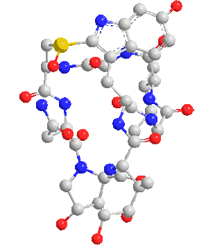
Materials that have nanometer size in all three dimensions and have no dimensions of freedom. According to some classifications, this category of nanostructures is also called nanoparticles. Factors affecting the properties of nanoparticles are the size and type of particles.

Conclusion:
The ability to produce large micro- and nanostructures on non-planar surfaces is important for many applications such as optics, optoelectronics, nanophotonics, imaging technology, NEMS, and microfluidics. However, it is very difficult to create large nanostructures on curved or non-planar surfaces using existing patterning methods.
Researcher and author: Dr. ( Afshin Rashid)
Specialized doctorate in nano-microelectronics