Nano-lithography techniques (optical and electron beam) periodic up to 50 nanometers (PhD in nano-microelectronics)
Researcher and author: Dr. ( Afshin Rashid)
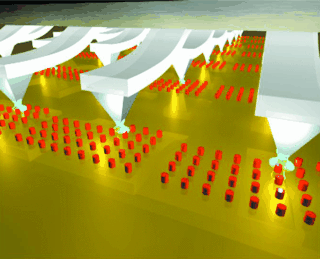
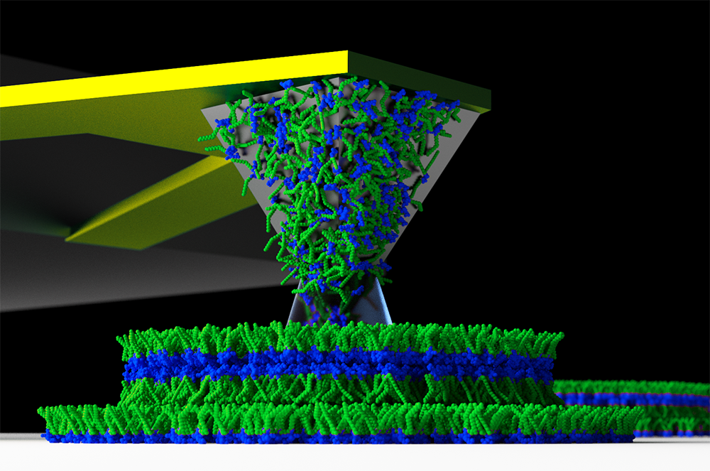
Note: Periodic nan lithography techniques (optical and electron beam) up to 50 nanometers can remove materials directly without excessive use of resistors. As a direct nano-lithography method, the number of processing steps is minimized compared to other methods.
Nano-lithographic techniques (optical and electron beam) periodically up to 50 nm as a sequential nanolithographic technique are inherently slow and have much less throughput than various techniques and widely used liquid metal ion source based on nanomaterials. The most common type of source in nano-lithography equipment (optical and electron beam) is periodically converted to 50 nanometers . In recent years, however, new developments in sources such as gas field ion sources, plasma sources, and metal alloy sources are the next step in terms of clarity or power.
Because the ion-matter interaction is stronger than the electron-matter, it can have detrimental effects on the residual material and alter its physical and chemical properties. Important but key applications for nanotechnology technology (optical and electron beam) have been found in the semiconductor industry, nanotechnology, and materials science. Nano-lithographic sedimentation (optical and electron radiation) requires a gas injection system to localize a local precipitate from a precursor delivered in the form of a gas by separating the precursor created by appropriate radiation in the nanoelectric devices. Produce. The main advantage of this technique is the selective growth of a substance in the area of interest in one step. Due to the high resolution of nano-lithography technique (optical and electron beam) Sediments can be grown with high lateral resolution , but due to much less damage to the substrate due to the low linear motion of electrons compared to ions. In contrast, the growth rate and metal content in sediments generally give rise to nanolithography (optical and electron radiation) .
Conclusion :
Nano-lithographic techniques (optical and electron beam) periodic up to 50 nanometers are able to directly remove materials without excessive use of resistors. As a direct nano-lithography method, the number of processing steps is minimized compared to other methods.
Researcher and author: Dr. ( Afshin Rashid)
PhD in Nano-Microelectronics


