Electrical Nanostructures of Localized Surface Plasmon PhD Nano-Microelectronics
Researcher and author: Dr. ( Afshin Rashid)
Note: In the structure of nanoplasmonic electrical nanostructures (surface plasmon) since the parameters of the material change significantly with frequency. In particular, this means that model experiments with, for example, microwaves and larger metal structures cannot replace experiments with metal nanostructures at optical frequencies.
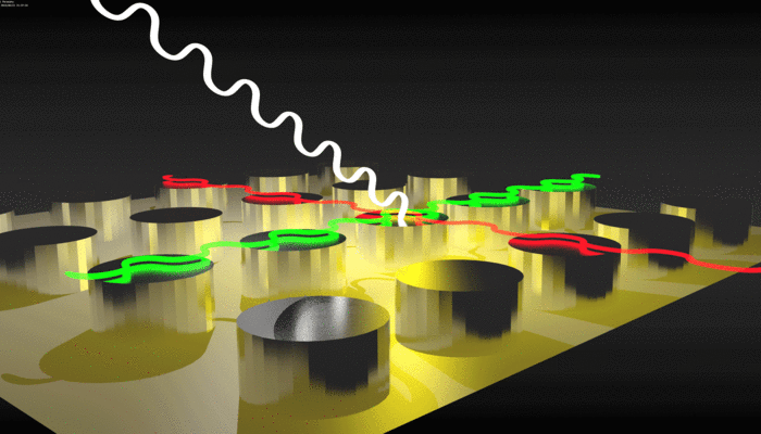
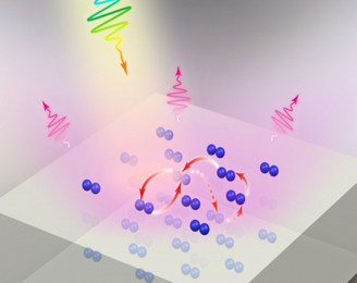
Surface charge density fluctuations associated with surface nanoplasms at the interface between a metal and a dielectric can cause highly near-light fields that are spatially enclosed near the metal surface. Similarly, if the electron gas is enclosed in three dimensions, such as a small particle, the general displacement of the electrons relative to the positively charged lattice results in a repulsive force, which in turn creates a specific particle-plasmon. Resonance depending on the geometry of the particle. In well-shaped particles (usually sharp), local charge accumulation associated with sharply increased light fields can occur. Alterations in some properties, such as conductivity in nanotransistors and electromagnetic properties in nanowires, may occur in dimensions of only a few nanometers.Patterning magnetic materials in arrays of nanoscale dots can lead to very strong and very controllable changes in the polarization of light when the beam is reflected from the array. This discovery could increase the sensitivity of optical components for telecommunications and biosensors applications. The pairing between light and magnetism in the electrical nanostructures of Localized Surface Plasmon results from quantum nanoelectronic interactions. These interactions lead to optical magnetic effects that change properties, such as the axis of polarization or the intensity of light. Interactions between light and matter increase at the nanoscale. This is a key motivation in the field of plasmonics, which results in the interaction of light with metal nanostructures leading to the construction of nanoelectronic devices.
In the electrical structure of Localized Surface Plasmon nanostructures, a nanoparticle-sized metal nanoparticle acts much like an antenna for visible wavelengths. Such antennas for us in many everyday devices that work on much longer radio and microbial waves used a phenomenon called surface network amplification in which all the nanoparticles, small antennas, in unison in one They radiate arrays. The key is to assemble longitudinal-scale magnetic nano-antennas that correspond to the wavelength of the incoming light. In periodic arrays, nanoparticles strongly interact with each other and cause mass oscillations. Such behavior has already been observed in metal nanoparticles.
Conclusion :
In the structure of nanoplasmonic electrical nanostructures (surface plasmon) since the parameters of the material change significantly with frequency. In particular, this means that model experiments with, for example, microwaves and larger metal structures cannot replace experiments with metal nanostructures at optical frequencies.
Researcher and author: Dr. ( Afshin Rashid)
PhD in Nano-Microelectronics


