

Section (Self-organized electrical nanostructure)
Electronic DND (multidimensional flexible sTMD) self-organized electrical nanostructure in nanometer dimensions
Researcher and author: Dr. ( Afshin Rashid)
Note: The properties of sTMD flexible multi-dimensional materials in the dimensions of modern nano-semiconductors have caused a revolution in wide technologies such as electronics, lighting, solar energy and communications.
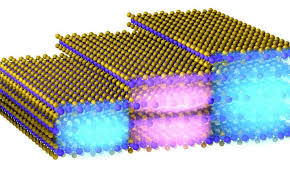
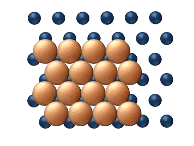
Most nanometals and metal nanoalloys, semiconductors, ceramics and some nanopolymers that have a crystalline structure have long-range order in their structure. The extent of this order between atoms or ions should be more than 100 nm. Atoms or ions are regularly repeated in three dimensions. Materials with long-range order are called crystalline materials. If a material has one large crystal, it is called a single crystal material.
Single crystal materials are suitable for many electronic and optical applications, for example, computer chips are made of single crystal silicon. Polycrystalline material consists of many small crystals in three dimensions. Monolayers are classified into H or T structures according to their stability, where H is the most common structure with TMD symmetry and trigonometric prismatic metal coordination, and T indicates a structure with multidimensional symmetry and octagonal metal coordination, and the structure are unstable.
In particular, single-layer TMDs of the multidimensional nanogroup are direct-gap semiconductors, while their thicker bilayers and multilayers have indirect gaps. For example, sTMD flexible multidimensional materials in nano dimensions all change from indirect to direct gap when passing from two layers to a cross layer. In general, the electronic structure of sTMD flexible multidimensional materials depends on the crystal phase and As a result, a wide range of electronic characters including metallic, semi-metallic, semiconductor and superconductors (SC) are created for flexible multidimensional materials of various sTMDs .

Conclusion:
The nano-microelectronics industry uses Si to make electronic circuits and GaAs, GaN and other III-V materials for nano-optical devices, with typical substrates consisting of wafers produced from sTMD flexible multidimensional materials at nanoscale temperatures . up Precisely controlled thin films can be deposited on the substrate to achieve additional functionalities, for example by chemical vapor deposition (CVD) or molecular beam epitaxy.
Researcher and author: Dr. ( Afshin Rashid)
Specialized doctorate in nano-microelectronics