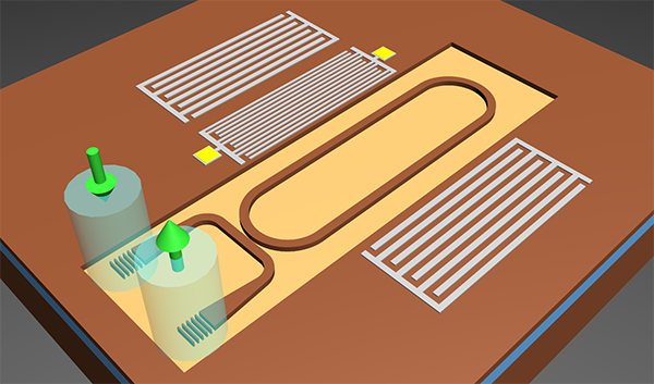
Nano-optical-electronic elements use microstructures that are one or more times smaller than the wavelength of the reflected light (PhD Nano-Microelectronics)
Researcher and author: Dr. ( Afshin Rashid)
Note: The size of the subwave structure is key to optical and optical benefits. Nano-optical elements use microstructures that are one or more times smaller than the wavelength of the incident light - their dimensions are usually between 10 and a few hundred nanometers. In such dimensions, these structures may interact with light both on the basis of classical optics principles and in the realm of relatively small-scale local interactions.
The exact application of the boundary conditions of the Maxwell equation describes the interactions of light with nanoparticle structures. For very small structures, single-electron or quantum effects may be observed. As a result, many nano-optical devices exhibit unique optical behaviors — such as high polarization differentiation in a thin micron space, chromatic phase lag, and monolayer combinations of optical functions such as polarization and spectral filtering. Whether accidentally or intentionally. These nano-optics offer useful alternatives to optical circuit design. Others can simply be designed as an alternative to classic bulk optics.
In addition to unique behaviors, devices also reach their optical effects at relatively short distances - nano-optical devices are generally very thin, usually one micron or less thick. This has strong positive implications for integrated optics because nano-optical structures can often be used as thin films as a "coating layer" during a complex manufacturing process. Single-electron and quantum effects also make optical performance easy to customize. Modifying the properties of materials by adding nanostructures leads to a continuous range of optical functions - essentially creating a combination of synthetic and optical materials - which allow the properties and wavelengths of light to gradually and accurately fit Specify the specific needs of the program. Nano-optical structures can be realized through a variety of production methods. In terms of commercial utility, an optical device is not optimally functional unless it can be produced in large volumes, in a variety of different applications, and easily integrated with other related technologies. The first criterion is essential to achieving economies of scale. Second, to ensure that the market opportunity is wide enough to be interesting. And third, to facilitate easy integration of nanoparticles into more complex systems. Existing manufacturing methods (self-assembly and nano-lithography) achieve these goals to varying degrees. Some materials can create regular, nanoscale structures under well-controlled conditions - self-assembly. The problem with this approach is the inflexibility of achievable structures and usable materials that limit achievable performance. Nano-lithography, which is similar to the production of standard semiconductors, generally uses some methods to create an image in the polymer resist layer.
Conclusion :
Sub-wavelength structure size is key to optical and optical benefits. Nano-optical elements use microstructures that are one or more times smaller than the wavelength of the incident light - their dimensions are usually between 10 and a few hundred nanometers. In such dimensions, these structures may interact with light both on the basis of classical optics principles and in the realm of relatively small-scale local interactions.
Researcher and author: Dr. ( Afshin Rashid)
PhD in Nano-Microelectronics


