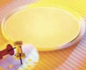
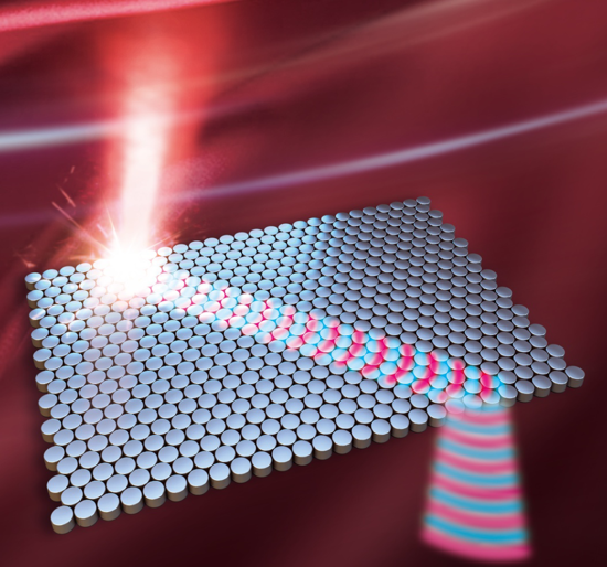
Nano-optical wafers are produced using nano-lithography process on wafers with a diameter of 100 or 150 mm. Nano-optical chips are made from micro wafer (PhD in Nano-Microelectronics)
Researcher and author: Dr. ( Afshin Rashid)
Note: Some materials can create regular, nanoscale structures in well-controlled conditions - self-assembly. The problem with this approach is the inflexibility of achievable structures and usable materials that limit achievable performance.
Nano-lithography, which is similar to the production of standard semiconductors, generally uses methods to create an image in the polymer resist layer. This image is then used as an etch mask to transfer the nanoscale pattern to the target material. Nano-lithography methods include interference lithography, electron beam lithography (electron beam), and nano pattern repetition (see sidebar for definitions). In general, each of these methods is optimal for some nanostructure patterns, materials, and volumes required. As a production method, nano-lithography supports a wide range of integration modes for optical circuits.
Integrated optical devices and sub-assemblies based on nano-optical elements realize various advantages. Compared to conventional bulk optics, their size and optical properties make the alignment in the assembly more generous, less carter and less expensive. When physically combined with other nano-optics or other materials in production to create a seamless integrated optics, this eliminates the complications and laminating costs of multiple devices while increasing reliability. Also, array nano-devices can be used in multi-beam or multi-path optical circuits, eliminating the need for separate discrete optics alignment. In general, the manufacturing process of nano-optical elements is flexible and robust, which saves on the cost of the manufacturing process in creating composite and integrated optics. Again, the resulting light is often smaller, stronger, more practical, and easier to collect. Because nano-optical devices are manufactured using wafer-based processes developed in semiconductor fabrication, this provides flexible sharing capacity in production capacity and supports high-volume production capacity. .
Nano Optics uses a growing "design vocabulary" that is functionally equivalent to the design libraries used in semiconductor applications. Multiple design elements can be used with complex, multi-step, and multi-process methods to create complex nanotubes and multilayer devices. The wide range of different nanostructure patterns, materials and integration methods means that there are no inherent limitations in the performance and operating wavelength of nanoparticle devices. These features are guided only by the needs of the program and the optical circuit.
Conclusion :
Some materials can create regular, nanoscale structures in well-controlled conditions - self-assembly. The problem with this approach is the inflexibility of achievable structures and usable materials that limit achievable performance.
Researcher and author: Dr. ( Afshin Rashid)
PhD in Nano-Microelectronics


