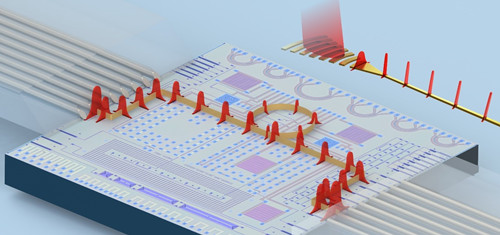
There are no inherent limitations in the performance and operating wavelength of nano-electro-optical devices. These features are guided only by the needs of the program and the optical circuit (PhD Nano-Microelectronics)
Researcher and author: Dr. ( Afshin Rashid)
Note: Nano Optics uses a growing "design vocabulary" that is functionally equivalent to the design libraries used in semiconductor applications. Multiple design elements can be used with complex, multi-step, and multi-process methods to create complex nanotubes and multilayer devices.
The wide range of different nanostructure patterns, materials and integration methods means that there are no inherent limitations in the performance and operating wavelength of nanoparticle devices. These features are guided only by the needs of the program and the optical circuit. Integrated optical devices and sub-assemblies based on nano-optical elements realize various advantages. Compared to conventional bulk optics, their size and optical properties make the alignment in the assembly more generous, less costly and less expensive.
When physically combined with other nano-optics or other materials in production to create a seamless integrated optics, this eliminates the complications and laminating costs of multiple devices while increasing reliability. Also, nano-array devices can be used in multi-beam or multi-path optical circuits, eliminating the need for separate discrete optics alignment. In general, the manufacturing process of nano-optical elements is flexible and robust, which saves on the cost of the manufacturing process in creating composite and integrated optics. Again, the resulting light is often smaller, stronger, more practical, and easier to collect. Because nano-optical devices are manufactured using wafer-based processes developed in semiconductor fabrication, this provides flexible sharing capacity in production capacity and supports high-volume production capacity. . Through the right combination of materials and structures, nano-optical devices can perform any passive optical function, including polarization filter, phase lag, spectral filter, and emission management (e.g., lenses and beam splitters). Various functions can be designed for open and wave based applications. Nano-optical devices can also be designed to operate in any wavelength range. The main method can be used for UV, visible and IR wavelengths with appropriate changes in dimensions and structural materials. In addition, they can form the core of an optical system. Practical applications of nano-optics require a complete optical system consisting of nano-patterned materials and adjacent materials including optical substrates and thin film coatings. Nano-optical structures are defined as a combination of material and physical properties.
Conclusion :
Nano Optics uses a growing "design vocabulary" that is functionally equivalent to the design libraries used in semiconductor applications. Multiple design elements can be used with complex, multi-step, and multi-process methods to create complex nanoparticles and multilayer devices.
Researcher and author: Dr. ( Afshin Rashid)
PhD in Nano-Microelectronics


