

Department of Nano Electronic Memory Laboratory
Testing of N_RAM nano electric memories
Researcher and author: Dr. ( Afshin Rashid)

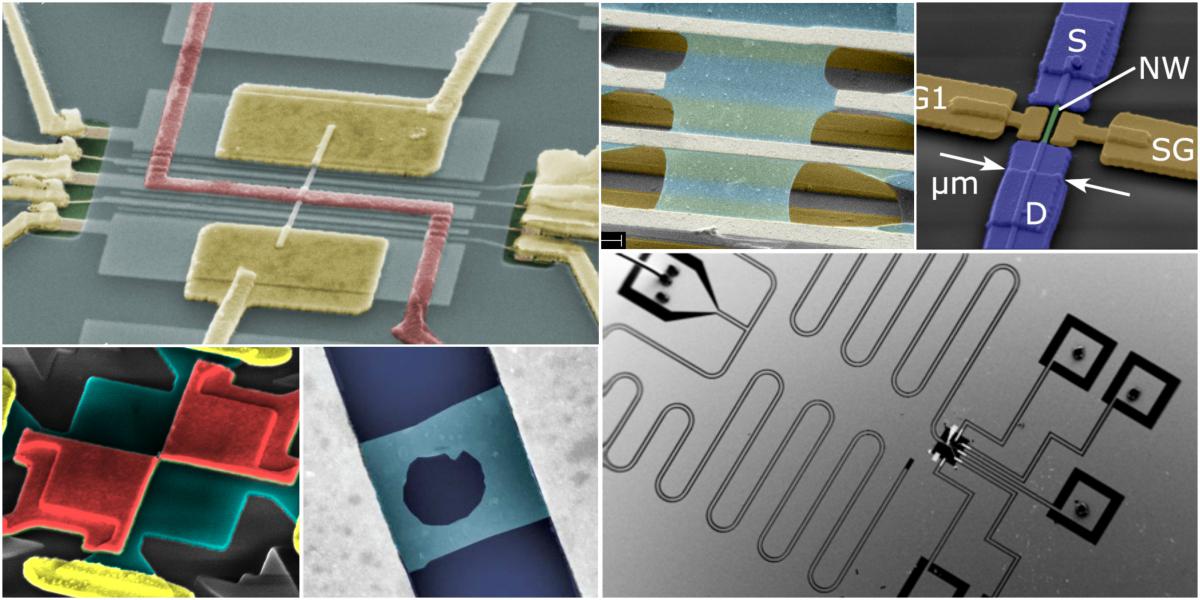
Note: The dielectric nano layer is a barrier between positive and negative charges, which has a very small thickness. And the nano material is also an electrolyte that contains positive and negative ions. By placing a potential between the electrodes of the capacitor, negative ions move towards the positive electrode and positive ions move towards the negative electrode. Finally, two capacitors connected in series are obtained.
Support nanostructures (NRAM multipurpose memories) are made of memory chips made of carbon nanotubes, although the discovery of small but very resistant, flexible and conductive carbon nanotubes with dimensions equal to DNA strands and the use of Chlorophyll-like small organic molecules can be absorbed instead of charge storage capacitors in DRAM and NRAM type memory chips. Nano crystals, the use of which will increase the lifespan of flash memories. and the development of a kind of magnetic material based on ferritin protein that will be used in the manufacture of disk drives and memory chips.Production and manufacturing of memories is one of the largest industrial sectors, but it also faces many technical problems; Problems such as charge leakage from the capacitor, structures with increasing complexity, and sensitivity to minor errors caused by cosmic rays. The existence of such problems makes chip manufacturers unable to reduce the dimensions of their chips more than this. Other significant issues in this field include SRAM chips related to large memory cells, the difficulty of placing DRAM and flash memory next to logic chips, and the slow access time of flash memory and its limited stability.

Each quantum dot consists of a single ball of several hundred atoms that can have one of two magnetic states. This allows them to contain a single bit of information (zero or one), as is customary in machine computing. In conventional hard disks, the data bits must be spaced far enough apart that they do not overlap. Quantum dots act as completely independent units that are not structurally connected, so they can become somewhat closer to each other.

Conclusion :
The dielectric nano layer is a barrier between positive and negative charges, which has a very small thickness. And the nano material is also an electrolyte that contains positive and negative ions. By placing a potential between the electrodes of the capacitor, negative ions move towards the positive electrode and positive ions move towards the negative electrode. Finally, two capacitors connected in series are obtained.
Researcher and author: Dr. ( Afshin Rashid)
Specialized doctorate in nano-microelectronics