

Department of Nano Electronic Memory Laboratory
Reproduction (electrical nano-memory) by combined nano-lithography (12 V), fast switching speed (1 microsecond)
Researcher and author: Dr. ( Afshin Rashid)

Note: The resulting graphene nano-memories are molecularly developed, offering superior programmable nano-scale memory performance compared to previous graphene memory devices and a large memory window (12 V), fast switching speed (1 μs). , shows strong electrical reliability.
Graphene molecular nanomemories show unique electronic properties, and its small dimensions, structural strength, and high performance make it very promising as a charge storage medium for nanomemory applications. We present a series of techniques using a nanoparticle solution, which creates a very thin layer on the target substrate and is used as a sacrificial layer during the nanopatterning process.
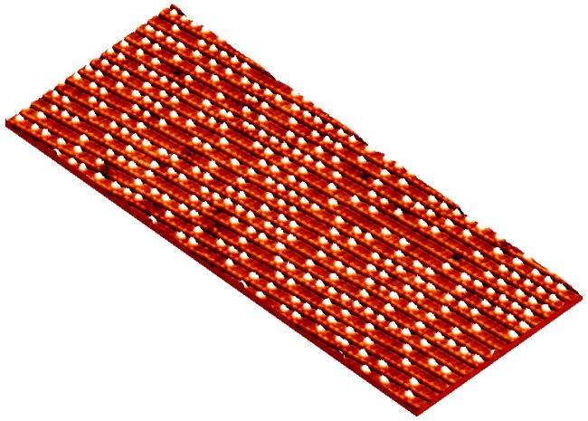
Due to the interaction between nanoparticles, they can organize themselves and create a thin layer that creates holes between them, this technique was originally called natural lithography . Due to the integral nature of colloidal particles and their hydrophilic character, they form a colloidal crystal with ordered cavities through which the substances of interest penetrate and deposit on the substrate. For example, polystyrene latex nanospheres can be used. Materials deposited on nanoparticles disappear after immersing the sample in a suitable solvent and sonication. This process is similar to a removal process . The advantages of this technique include wide patterns, simplicity, good resolution, and the ability to combine with other lithography techniques. On the other hand, this technique creates problems due to the limited forms available for patterned functional materials, the range order of nanopatterns and the existence of point defects. Hybrid nanolithography has also been used to perform successive exposures of chemically enhanced resists by optical lithography and electron beam lithography. Oriented block copolymer nanolithography is a combination of top-down lithography and bottom-up self-organization of two polymers. to produce nanopatterns with high resolution in large areas . Typically, block copolymer self-organization is randomly oriented and lacks long-range order , but the previous top-down pattern provides the substrate for oriented block copolymer lithography. , combined nanolithography irradiation of a substrate causes preferential growth of semiconductor materials in the irradiated regions, which can be used to fabricate ordered arrays of semiconductor dots.

Conclusion :
The resulting molecularly developed graphene nano-memories provide excellent programmable nano-scale memory performance compared to previous graphene memory devices and a large memory window (12 V), fast switching speed (1 μs), capability It shows strong electrical reliability.
Researcher and author: Dr. ( Afshin Rashid)
Specialized doctorate in nano-microelectronics