Bonding of nanostructures Nano structure and nanotransistors (PhD in nano-microelectronics)
Researcher and author: Dr. ( Afshin Rashid)
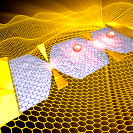
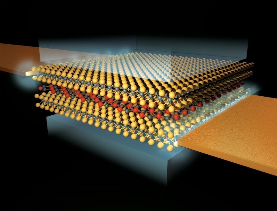
Note: Nanostructures Nano structure The electronic properties of two regions are "protected" differently by a special, so-called topological, method, and thus, a very strong new quantum state is created in the transition region.
This local electron quantum state can now be used as a primary property for the production of special semiconductors, metals, or insulators - and possibly even as a feature in nanoelectronics. The shapes and sizes of nanostructures are naturally determined by their composition and formation conditions. The properties of nanostructures, in turn, determine the originality of the properties of nanostructures and the possible contexts of their operation . The range of 1 to 1000nm is introduced as the range of nanostructures, an important feature of nanostructures is the control of the organization's own processes. The range of change in nanostructure activity depends on the nature and shape of the nanostructure. With However, if the energy field of nano-energy electromagnetic radiation is comparable if certain range Wavelength changes dramatically with the occurrence of chemical reactions in irradiated materials. The activity of nanoparticles will be significant up to 100 nm.
Nano-Microelectronics is developing new methods for making nanotransistors on a small scale, measuring several tens of nanometers, which is derived from a science called nanotechnology. Unlike today's nanotransistors, which behave based on the mass motion of electrons in matter, new devices follow the phenomena of nanoscale quantum mechanics in which the discrete nature of the electron can no longer be ignored. By shrinking all the horizontal and vertical dimensions of the transistor, the electric charge density in the various regions of the nanotransistor increases, or in other words, the number of electrical charges per unit area of the nanotransistor increases. This has two negative consequences : First, by increasing the density of the electric charge, the possibility of discharging the electric charge from the insulated areas of the transistor increases. And this causes damage to the transistor and its failure. This is similar to the discharge of excess electric charge between the cloud and the ground in the phenomenon of lightning, which ionizes air molecules into negative and positive ions. Second , as the density of the electric charge increases, the electrons may move out of the radius of one atom and into the radius of the adjacent atom under the influence of the momentum or abduction forces that have now increased. In quantum physics, this is called tunneling. Electron tunneling from one atom to an adjacent atom is a phenomenon that occurs on a small scale between electrons. This phenomenon is the basis of some electronic components and some nanoscopes. But in nanotransistors this is not a useful phenomenon, because it is possible to tunnel electrons from one atom to an adjacent atom. Is to continue and cause an electric current. Although this electric current may be very small, because it is unintended and unpredictable, it acts as a leakage path for the electric current and changes the electrical behavior of the nanotransistor.
Conclusion :
Nanostructures Nano structure The electronic properties of two regions are "protected" differently by a special method, the so-called topology, and thus, a very strong new quantum state is created in the transition region.
Researcher and author: Dr. ( Afshin Rashid)
PhD in Nano-Microelectronics


