Behavior and electromagnetic absorption of cobalt nanowires (based on PhD in nano-microelectronics)
PhD in Education and Research
Researcher and author: PhD student Afshin Rashid
Note: Cobalt nanowires exhibit electromagnetic absorber behavior at moderate temperatures, and when a magnetic field perpendicular to the nanowires is applied, these nanoelectronic devices have a larger induction field than when the electromagnetic field is parallel. Forms in cobalt nanowires.
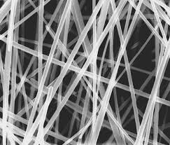
Nanowires have a structure that has an amazing length-to-width ratio . Nanowires are very thin - it is possible to create nanowires with a diameter of only one nanometer, nanowires are used to create the smallest transistor (nanotransistors). Nano wire Nano wire can have insulating, semiconductor or metal properties . Insulators do not withstand electrical charges, while metals have very good electrical charges. The semiconductors are located between the two and are charged under suitable conditions. By placing the semiconductor wires in the proper configuration, transistors can be made that act either as switches or amplifiers .Some of the interesting and anti-flexible properties of nanowires are due to their small scale.
The technology of cobalt nanowires in the approximate dimensions of 1 to 100 nanometers, where only one of its kind phenomena offers descriptive applications, is material. Nanotechnology encompasses science, engineering, and non-scale technology, imaging, measuring, designing, and manipulating materials at this length scale. Due to nanotechnology, computers have become faster than before and the value of computing has decreased. In the immersion method, nanowires have enough time to transfer from nanoparticle particles to cavities ; The formation step of uniform nanoparticles is done slowly and finally uniform nanowires are formed. Structural study with FESEM in the immersion method of single-stranded nanowires in all porosities and in a large area of nanowire particles are formed. The simple answer to this question is that each particle is less than 100 nanometers. But like The scale from 1 to 100 nm determines the size range of a nanoparticle. In order to prevent the contact of cluster particles from atoms, less than 1 nm may be removed, but the movement of electrons in nanoparticles to particles is <1 nm. Because the particles are three-dimensional.
Conclusion :
Cobalt nanowires show the behavior of an electromagnetic absorber at a moderate temperature, and when a magnetic field perpendicular to the nanowires is applied, these nanoelectronic devices have a larger induction field than when a parallel electromagnetic field is applied to the nano. Cobalt wires are formed.
Author: PhD student ( Afshin Rashid)


