Graphene-based FET nano-transistors (based on nano-microelectronics) (educational-research doctorate)
Researcher and author: Dr. ( Afshin Rashid)
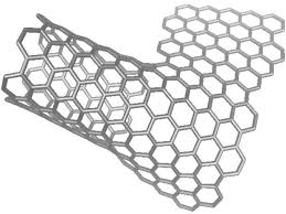
Note: Graphene nano material is a honeycomb-like material with a thickness of one carbon layer due to its properties such as high mobility of electrons and holes and thermal and mechanical stability, used in the nanoelectronics industry and the manufacture of graphene nano-transistors. FET was exposed.
Although graphene is a semiconductor material with zero gap and is not suitable for logic circuits, using nanoelectronics technology creates different forms of this material for the production of graphene FET nano-transistors that have different gaps (2.1-0 eV). Graphene nano-strips, multilayer graphene and graphene grown on SiC to reproduce FET graphene nano-transistors such as these have had a significant impact on the design industry of new nanoelectronic devices. The field has a FET graphene tunnel that uses energy-free graphene without drainage in its drainage and source regions and in the catalytic domain of graphene with a narrow band gap (eV2 / 1). This structure has better electronic properties than the other two structures in which the three regions of the source channel and the drain are used in the first structure of graphene without energy band gap and in the second structure of graphene with energy band gap.
In the proposed structure, the rate reaches the appropriate rate that a FET graphene nano-transistor is suitable for digital structures and the output properties show a very good saturation state. In this study we have basic parameters such as doping concentration, drain voltage, dielectric thickness and differences between gate and graphene electrode working functions in three structures. This increases the doping effect on the current and increases it, which increases the doping rate of FET graphene nano-transistors, which are very suitable for use in low-power devices.
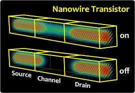
The term transistor comes from a combination of two words transfer and resistance. In a FET graphene nano-transistor, the resistance between two electrodes can be transmitted or controlled by a third electrode. Source coupling and drain coupling take place through a face semiconductor (graphene nano-layer). The gate nano-electrode is separated from the semiconductor by the electrical insulation of the gate dielectric layer. Thus, the gate nano-electrode binds to the semiconductor as a graphene layer and controls the electrostatic potential of the semiconductor / insulator interface .
Researcher and author: Dr. ( Afshin Rashid)


