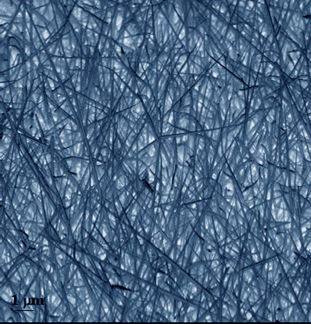
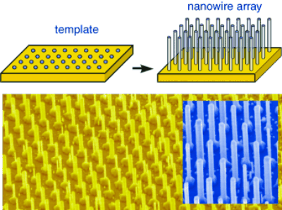
Structure and structure of semiconductor nanowires (NWs) based on nano- microelectronics PHD (educational-research doctorate)
Researcher and author PhD student : Afshin Rashid
Tip: Semiconductor nanowires (NWs) have attracted a lot of attention due to their physical properties for use in electronics and photonics. Nano wires are a thousand times thinner than human hair. And allows high-efficiency photon components to be propagated in nanoparticles.
The entry of semiconductor nanowires ( SiNWs) into optical detectors or solar cells is done by increasing the interaction of light-matter and its surface geometry. The porous semiconductor nanoparticles produced by this method have repeatable and acceptable optical properties. Among the factors influencing the structure and optical properties of these semiconductor nanoparticles (NWs) are the length of the nanowires and their diameter decreases.
NWs nano-wires are just like ordinary electrical wires, except that they are very small. NWs nano-wires are made in two ways: in the bottom-up process or the nanoscale growth method, and the semiconductor layers, the crystals grow to the desired structures. This process allows the electrical conductivity of the nanowires to increase during the conduction effect. NWs nano-wires can be used to connect small parts to very small circuits . Metal nanoparticles and insulators and semiconductors are the body of new advances in materials with a negative two-dimensional or three-dimensional index.
Conclusion:
Semiconductor nanoparticles (NWs) have attracted a lot of attention due to their physical properties for use in electronics and photonics. Nano wires are a thousand times thinner than human hair. And allows high-efficiency photon components to be propagated in nanoparticles.
Author: PhD Student ( Afshin Rashid)


