Classical application of nano-lithography for manufacturing integrated circuits and other nano-electronic devices (maximum 50 nm) (PhD in nano-microelectronics)
Researcher and author: Dr. ( Afshin Rashid)
Note: The classic application of nano-lithography is the fabrication of integrated circuits and other electronic devices in which optical lithography is widespread. In addition, various types of nano-lithography techniques are used in research activities with the aim of modeling materials and realizing prototypes and proof-of-concept devices.
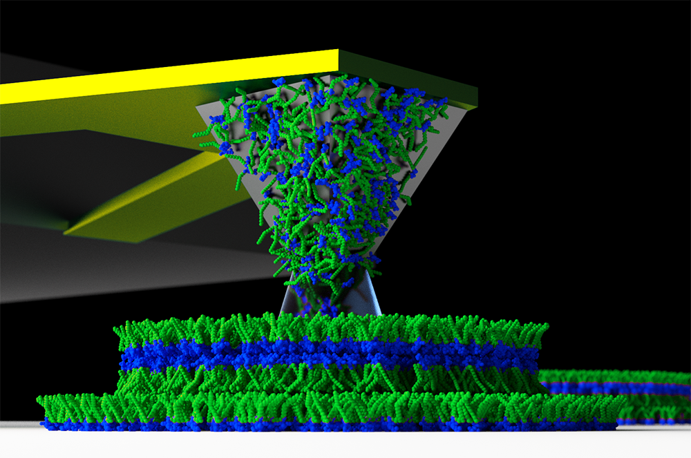
Classical application methods of nano-lithography on a spin substrate Due to the specific interactions between these polymers and the substrate , in certain conditions, two types of polymers tend to form an intertwined pattern, there is a local order between the two polymers and the range Forms such as nanowires with a period in the range of 50 nanometers. This pattern would be very useful if the subsequent application of the classic nano-lithography, which tends to accumulate on top of the polymer after landing on the layer due to less penetration mobility. Thus, the thin structure follows the polymer scaffold, which expands smoothly along different microns. However, the formed nanowires reveal some unwanted features as a closer lookSignificant unevenness is observed in the fabrication of nanowires, and the nanowires are cut at certain points and deviate from the straight shape, all of which are typically the source and deterioration of the physical properties of nanowires. In addition, long-distance ordering of fabricated nanowire arrays does not follow this strategy, which is essential in certain applications such as the semiconductor industry.
Due to the interaction between the nanoparticles, they can organize themselves and create a thin layer that creates holes between them, a technique originally called natural lithography . Due to the integration nature of colloidal particles and their hydrophilic properties, they form a colloidal crystal with arranged holes through which the material of interest penetrates and settles on the substrate. For example, polystyrene latex nanospheres can be used. The precipitated material on the nanoparticles disappears after the sample is immersed in a suitable solvent and sonicated. This process is similar to a removal process . The advantages of this technique include wide oligos, simplicity, good resolution and the ability to combine with other lithographic techniques. On the other hand, this technique creates problems due to the limited forms available for patterned applications, the arrangement of nanoparticles and the existence of point defects.
The classic application of nano-lithography is the fabrication of integrated circuits and other electronic devices in which optical lithography is widespread. In addition, various types of nano-lithography techniques are used in research activities with the aim of modeling materials and realizing prototypes and proof-of-concept devices.
Researcher and author: Dr. ( Afshin Rashid)
PhD in Nano-Microelectronics


