

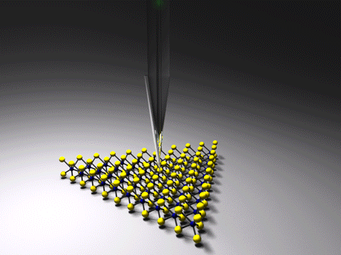
_process section (discharge) for electrical nanotubes
Resonance Raman spectroscopy (RAMAN) for electronic abundance measurement SWCNTs nanotubes
Researcher and author: Dr. Afshin Rashid
Note: It is very common to use this method to measure the abundance of nanotubes in a sample. In this technique, when the laser energy is equal to or close to the allowed optical electron transfer energy of the sample, we will have an increase in intensity, which is highly dependent on the sample's nano-electrical structure.
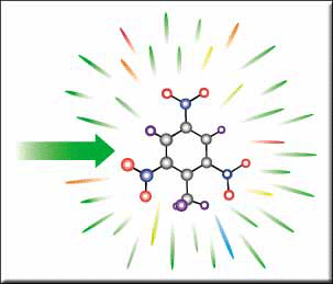
In the RRS of carbon nanotubes, even the Raman of a single nanotube is observed. The Raman spectrum of a single nanotube makes it possible to more accurately estimate the electronic and phonon structure of SWCNTs. Each carbon nanotube (m,n) has a special electronic structure and, as a result, the density of its special levels. 6> had So RRS is great for determining their structure. Nanotubes whose diameter 0/75nm<dt< 2.4nm SWNTs (type of SWCNTs), RBM Raman spectra between them (100cm- 1 <WRBM< 300cm) is the equivalent of the symmetric displacement within the phase of carbon atoms SWCNT in the radial direction. band G is related to the movement of neighboring atoms in opposite direction along the tube surface in graphite two-dimensional, which is characteristic It is a peak with several branches around (1500-1600cm). Peak related to RBM and multiple peak of band G is not seen in SP2. Usually no carbon compounds SP2 are a peak compounds that contain single carbon band G) is observed in the form of Lorentzian around (1-1582 cm) of their Raman spectrum. band D in the Raman spectrum only for SP2 atoms in the presence of (hetero) atoms, carbon spaces Empty or any network defects are created.
all these peaks in the Raman spectrum are sensitive to the SWCNT structure (indices m,n). Of course, the sensitivity of RBM is higher and therefore is used for initial identification (m,n). (band G) is also sensitive to the electronic structure. G band and RBM are widely used to arrange nanotubes. Raman spectroscopy using the number Many laser lines, accurate diameter distribution can be obtained, and finally more accurately the type of metal and semiconductor determined SWCNT. It has been determined that the G band of metal and semiconductor nanotubes is different. In graphite, the band G is a single peak because the in-plane tangential vibrations are degenerate from the planar hexagonal structure. while in nanotubes, this peak breaks into six peaks, which is due to the curvature of the graphene sheet and the quantum limitation 19> is along the pipe.
considering only two of breaking extreme peaks and analyzing them, which basically vibration symmetry Tangentity is obtained when the graphene sheet is rolled to form the shape of the cylinders of the tube. Appropriate information can be obtained. Two of the strongest G peaks are named +G to change the positions of -G. -G with lower frequency atom along the axis of the tube and to change the atomic position in the circular direction definition have been The difference between metal G-band (SWCNTs) and semiconductors is proof of this. The peak of metal nanotubes is wider and more asymmetric than semiconductors and shifts to low frequencies.

Conclusion :
Semiconductor nanotubes can be turned on/off in coordination with the device for voltage regulation. To distinguish metallic and semiconducting SWCNTs using V-I diagrams have been presented. These researchers hypothesized that semiconductor SWCNTs; have an off/on ratio of 10 or more and the off current is (9A-10) or less have that this issue is contrary to the characteristics of metallic SWCNTs. In addition, for enriched samples, four-point assays for thin films such as (paper bucky)