

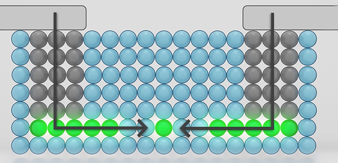
Source and drain connection in one (CNTFET nanotransistor) Schottky Dam (SB)
Researcher and author: Dr. ( Afshin Rashid)
Note: The connection between carbon and metal nanotubes used to connect the source and drain in a CNTFET forms the Schottky barrier (SB). The formation of Schottky dams in the source and drain of a transistor causes a significant reduction in the input current in this transistor. Therefore, for higher operational efficiency of CNFET components, suitable metals are needed that can be used at the junction of the sur and drain and create an ohmic connection .
When an electric field is applied to a CNTFET nano-transistor, the carbon nanotube between the source and the drain contains a moving charge. The density of these loads is for the source, and this density is determined by the probability of a Dirac form distribution. The ability of carbon nanotubes to be used in gas sensors is due to their hollow and high contact surface. This contact surface consists of the outer wall of the nanotube and its empty middle parts. Physico-chemical adsorption of gases in nanotubes changes their conduction. Lack of precise control over the positioning of CNTs when making CNFETs causes irregularities in nanotubes, less than half a percent of nanotubes made on a single diamond crystal substrate are irregular. Irregular nanotubes may cause a short circuit between the output and the feed.
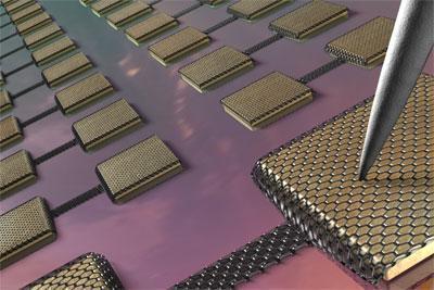
Due to the reduction in the scale of semiconductor components and integrated circuits to the nanometer range, the semiconductor industry will face many challenges. Reducing the scale causes more short channel effects, less gate control, increased exponential leakage currents, drastic process changes, and unmanageable power densities . CNTFET is an option for transistors in order to be able to continue reducing the dimensions and for the development of new structures, transistors are the field effect of carbon nanotubes. One of the most important issues in nanotechnology is carbon nanotubes. By shrinking all the horizontal and vertical dimensions of the transistor, the electric charge density in the various regions of the nanotransistor increases, or in other words, the number of electrical charges per unit area of the nanotransistor increases. This has two consequences Negative: First, by increasing the density of the electric charge, the possibility of discharging the electric charge from the insulated areas of the transistor increases, and this event causes damage to the transistor and its failure. This is similar to the discharge of additional electrical charge between the cloud and the ground in the phenomenon of lightning, which ionizes air molecules into negative and positive ions. Second , as the density of the electric charge increases, the electrons may move out of the radius of an atom and into the radius of the adjacent atom under the influence of the momentum or abduction forces that have now increased. In quantum physics, this is called tunneling. Electron tunneling from one atom to an adjacent atom is a phenomenon that occurs on a small scale between electrons. This phenomenon is the basis of some electronic components and some nanoscopes. But in nanotransistors this is not a useful phenomenon, because the tunneling of electrons from one atom to an adjacent atom may continue and cause an electric current. Although this electric current may be very small, because it is unintended and unpredictable, it acts as a leakage path for the electric current and changes the electrical behavior of the nanotransistor.

Conclusion :
The connection between the carbon and metal nanotubes used to connect the source and the drain in a CNTFET forms the Schottky barrier (SB). The formation of Schottky dams in the source and drain of a transistor causes a significant reduction in the input current in this transistor. Therefore, for higher operational efficiency of CNFET components, suitable metals are needed that can be used at the junction of the sur and drain and create an ohmic connection .
Researcher and author: Dr. ( Afshin Rashid)
PhD in Nano-Microelectronics