

Tubular nanotransistors (3D 3D) Very high electron movement in graphene
Researcher and author: Dr. ( Afshin Rashid)
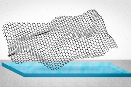
Note: Due to the very small thickness of graphene, it is possible to greatly reduce the gate length in field-based (ballistic bipolar nanotransistors) without dealing with the common problems in 3D nanotransistors.
In 3D tubular nanotransistors, the very high electron movement in graphene promises a threshold frequency as well as greater mobility in the circuit. The main advantage of two-dimensional ballistic bipolar transistor devices in the power processing criterion is their very small and desirable delay , which according to calculations reaches below 10fJ. Apart from graphene, other materials with a two-dimensional structure have been discovered, including silicon and germanium . Ideas have also been given for making 3D field nanotransistors using phosphor and graphene . But the conventional field-effect 2D ballistic nanotransistors that have been made so far are very slow and have a switching time of a few tenths of a millisecond, which limits their use to frequencies of a few kHz.Apart from bipolar ballistic nanotransistors and the common field effect, there are other ideas for using graphene or other two-dimensional materials in the construction of transistors . One of these ideas is the 3D nanotransistor of tunnel field effect, which has the desired speed up to several GHz, low power consumption and more current changes in the drain are the advantages of this transistor. There are also other nanodevices with gate voltage in the sub-threshold area, such as ballistic dipole transistors, as well as optical devices based on graphene or other available two-dimensional materials.
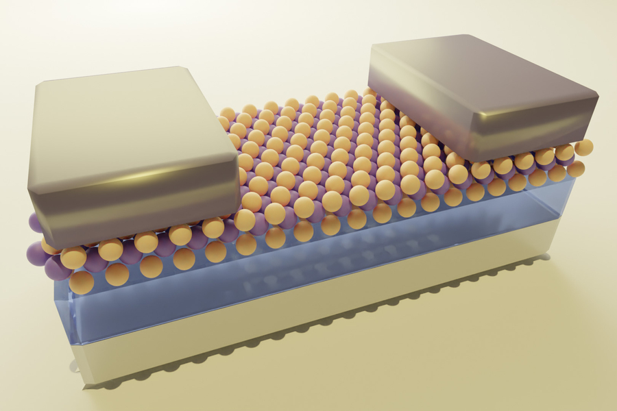

3D nanotube transistors are tubes with a graphene wall. These pipes, as in the structure, can be single-walled or multi-walled. On the other hand, depending on how the carbon atoms are wrapped and arranged at the edge of the tube, they are found in three forms (chair handle, zigzag and tube-like chiral) . These three forms of carbon nanotubes have very different properties. For example, the seat handle structure behaves like a metal conductor, while the chiral nanotube structure behaves like a semiconductor , combining this function with a small adaptation of the gap energy to 3D carbon nanotubes. It also gives unique electrical and mechanical properties to 3D tubular nanotransistors. The main problem in using nanotubes in the construction of 2D ballistic nanotransistors is mainly that they must be used lying on the surface to be connected to them and a metal connection can be established to achieve the behavior of the transistor. Vertical nanotubes, on the other hand, grow faster in the proliferation of ballistic 2D nanotransistors. If the semiconductor and metal nanotubes are assumed to be able to grow and orient on the surface with the desired accuracy, they will be able to compress and increase the speed of the integrated electronics as much as possible.

Conclusion :
Due to the very small thickness of graphene, it is possible to greatly reduce the gate length in field-based (ballistic bipolar nanotransistors) without dealing with the common problems in three-dimensional nanotransistors.
Researcher and author: Dr. ( Afshin Rashid)
PhD in Nano-Microelectronics