

5 nm transistor generated (basic Si / SiGe heterostructure)
Researcher and author: Dr. ( Afshin Rashid)
Note: Changes in the channel width of the nanotransistor around the gate field effect can cause undesirable changes and loss of mobility.
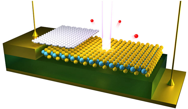
A gate nanotransistor - the gateway around the FET - can bypass the problem. And electrostatically, the gate gate is a versatile nanotransistor in which a gate is placed on all four sides of the channel. It's basically a silicon nanowire that the universe revolves around. In some cases, the surrounding FET may have a common gate or other material in the ducts. Horizontal layer nanotubes appear as the consensus for the 5 nm transistor. These devices start with alternating layers of silicon and silicon germanium (SiGe) that are patterned into columns. The initial heterostructure of Si / SiGe is explicit and the columnar pattern is similar to the fin structure for nanotransistors. Several for GAAFET nano sheet transistors The indentation in the SiGe layers creates an internal distance between the source / discharge, which ultimately sits next to the column and the space at the gate of the nanotransistor gate. This distance determines the width of the gate opening. It then removes a free SiGe channel etch when internal distances are in place. The nanoelectric layer places the gate and the metal in the spaces between the silicon nanowires. To minimize lattice distortion and other defects, the germanium content of SiGe layers should be as low as possible. The choice of nanoplayers in the surrounding gate transistor nanotransistors increases with the content of Ge or germanium, and the erosion of the silicon layers during indentation or channel channel release of the transistor and channel release affects the thickness of the surrounding gate channel and thus the threshold voltage. Put.


By shrinking all the horizontal and vertical dimensions of the transistor, the electric charge density in the various regions of the nanotransistor increases, or in other words, the number of electrical charges per unit area of the nanotransistor increases. This has two negative consequences: First, by increasing the density of the electric charge, the possibility of discharging the electric charge from the insulated areas of the transistor increases , and this event causes damage to the transistor and its failure. This is similar to the discharge of excess electrical charge between the cloud and the ground in the phenomenon of lightning, which ionizes air molecules into negative and positive ions. Second , as the density of the electric charge increases, the electrons may move out of the radius of an atom and into the radius of the adjacent atom under the influence of the momentum or abduction forces that have now increased. This What happens in quantum physics is called tunneling. Electron tunneling from one atom to an adjacent atom is a phenomenon that occurs on a small scale between electrons. This phenomenon is the basis of some electronic components and some nanoscopes. But in nanotransistors, this is not a useful phenomenon, because the tunneling of electrons from one atom to an adjacent atom may continue and cause an electric current. Although this electric current may be very small, because it is unintended and unpredictable, it acts as a leakage path for the electric current and changes the electrical behavior of the nanotransistor.

Conclusion :
Changes in the channel width of the nanotransistor around the gate field effect can cause undesirable changes and loss of mobility.