

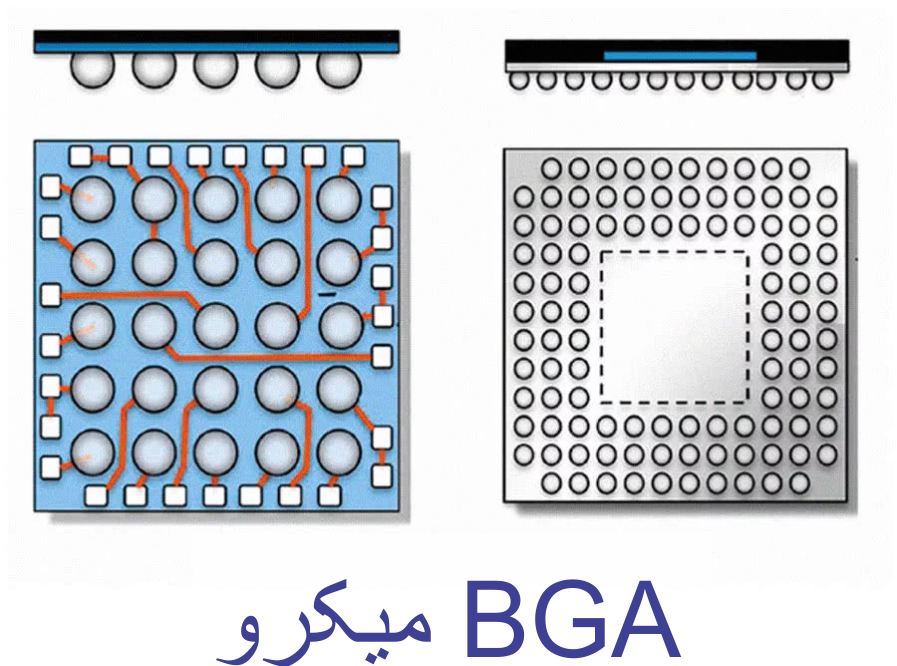
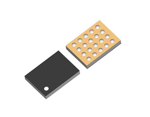
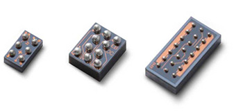
Micro BGA or Micro BGA section
Micro BGA of WLP / CSP type (a type of micro BGA processor)
Researcher and author: Dr. ( Afshin Rashid)
Note: CPU or Central Processing Unit is the main hardware of the computer. Its most obvious feature is performing logical calculations and information processing.
CPU is actually the central processing unit of any computer or server. Computers or tools that need to perform calculations cannot do anything without the CPU, the CPU receives the information from the memory, then applies various algorithms such as multiplication and addition or logical operations such as and or or or not on them and Finally, it delivers the output.

The more powerful the processor is, the more data it can process and the faster the system will be. All the different parts of the computer are dependent on the CPU and without it no operation can be done. But the CPU is not able to work alone and needs memory to store information, graphics processor to render images and thousands of other small and large parts. Over the years since the first CPUs were released, many improvements have been made. But despite this fact, the main function of CPU still consists of three simple steps: Fetch, Decode and Execute.
The measure of CPU speed is MHz. Each bit has a value of zero or one, which are processed by the CPU. In 32-bit processors, the amount of processing is equal to 4,294,967,295, while in 64-bit processors, this value is equal to 18,446,744,073,709,551,615.
Core processors or multi-core CPUs
In the beginning, CPUs had only one core. This means that the central processing unit was limited to perform only one set of tasks. This was one of the reasons why computers at the time, despite being impressive, were relatively slow and time-consuming.
After making a single core processor, manufacturers thought of ways to improve its performance. One of these ways led to the construction of multi-core processors. A dual-core processor simply means two separate CPUs on one chip. With the increase in the number of cores, CPUs were able to manage multiple processes simultaneously. This led to increased performance and reduced processing time. Dual-cores quickly gave way to quad-cores, and even octa-core processors followed. Today, thanks to Hyper-Threading, your computer can act as if it has 16 processing cores.
Researcher and author: Dr. ( Afshin Rashid)
Specialized doctorate in nano-microelectronics