

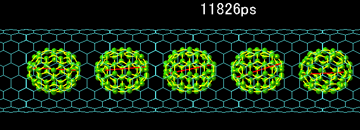
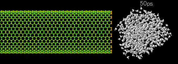
نکته : ساختار و خصوصیات الکترونیکی نانو لوله های تک جداره خالی (SWNT) و SWNT را که با مولکول های فولِرِنس پر شده است(nano peapods) نیز میگویند. خصوصیات این نوع از نانو لوله های SWCNT فلزی منحصر به فرد و به همراه الکترودهای فلزی یا منجر به ابر رسانا اختصاص یافته است.
nano peapods ها نانو لوله های کربنی هستند و مولکول های فولِرِنس را محاصره می کنند ، می توانند از نظر نانو لوله های CNT خالی عملکردی پیشرفته ارائه دهند. موارد کاربرد آنها ، به عنوان مثال ، دستگاه های ذخیره سازی داده ، ترانزیستورهای تک الکترون و آرایه های اسپین-کوبیت برای محاسبات کوانتومی را شامل می شود. نانو لوله توسط فولرین های به دام افتاده ، مانعی است که peapods بتواند در برنامه های الکترونیکی نانو مقیاس به تمام توان خود برسد.


نتیجه گیری :
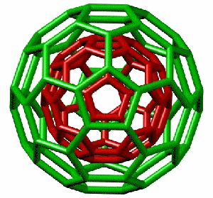
با یک اتصال نانو الکترومکانیکی بین حالت های الکترونیکی و کمی نانو لوله های کربنی CNT و لرزش های مکانیکی فولِرِنس ها میباشد. peapod کربن نانو مواد هیبریدی متشکل از کروی است. فولرین محصور در یک نانو لوله کربنی CNT. به دلیل شباهت آنها با بذر گیاه گیاه نخود نامگذاری شده است. از آنجا که خواص سنگهای کربنی با خصوصیات نانولوله ها و فولرها متفاوت است ، می توان peapod کربن را به عنوان نوع جدیدی از ساختار گرافیکی خود مونتاژ شده تشخیص داد.
پژوهشگر و نویسنده: دکتر ( افشین رشید)
دکترایِ تخصصی نانو _ میکرو الکترونیک