

Reverse bias in Darlington transistor = pair or pair (effect of voltage on base; collector; emitter)
Researcher and author: Dr. ( Afshin Rashid)
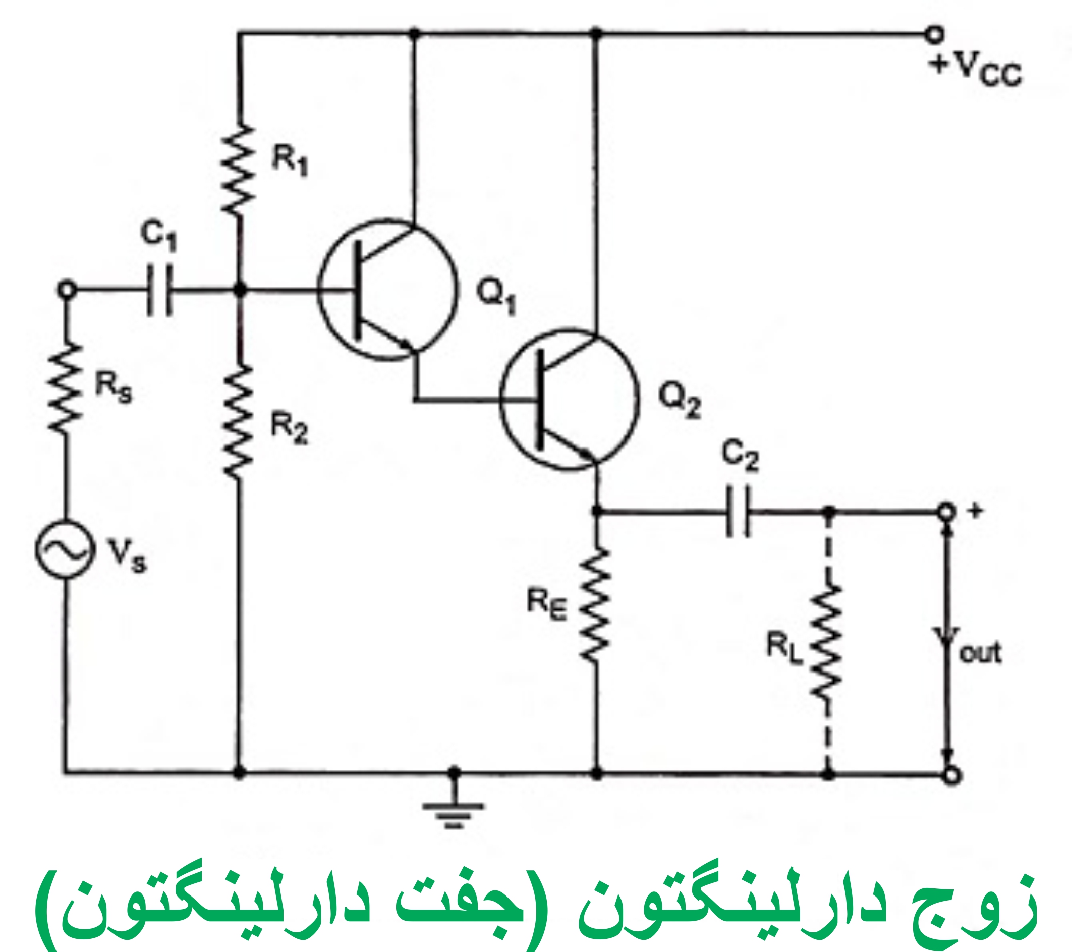
Note: Darlington transistor This seemingly voltage amplifier circuit has an interesting structure and function and is found in various types. The difference in the collector and emitter bases causes the reverse bias of the Darlington transistor .
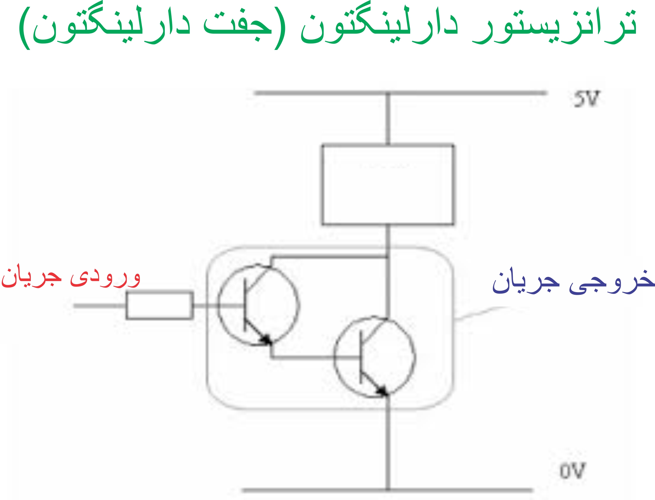
In the structure of the Darlington transistor, applying a voltage with the same polarity causes current to pass through a PN junction, and if the polarity of the voltage changes, no current will pass through the circuit. If we look at it simply, the function of a Darlington transistor can be considered as current amplification. Consider a small logic circuit that, under certain conditions, creates a very small current at its output. You can amplify this current with a Darlington transistor and then use this strong current to turn an electric relay on and off. There are also many cases where you use a Darlington transistor to amplify voltage. Obviously, this feature is directly inherited from the current amplification feature of this device. It is enough to put the amplified input and output current on a resistor so that the low input voltage is converted into an amplified output voltage.
_ife5.gif)
There must be a minimum input current that a Darlington transistor can amplify. If this current is less than the minimum, the Darlington transistor will not show any current at its output. But as soon as you increase the input current of a Darlington transistor to more than the minimum, you will see amplified current at the output. This property of the Darlington transistor is commonly used to make electronic switches.


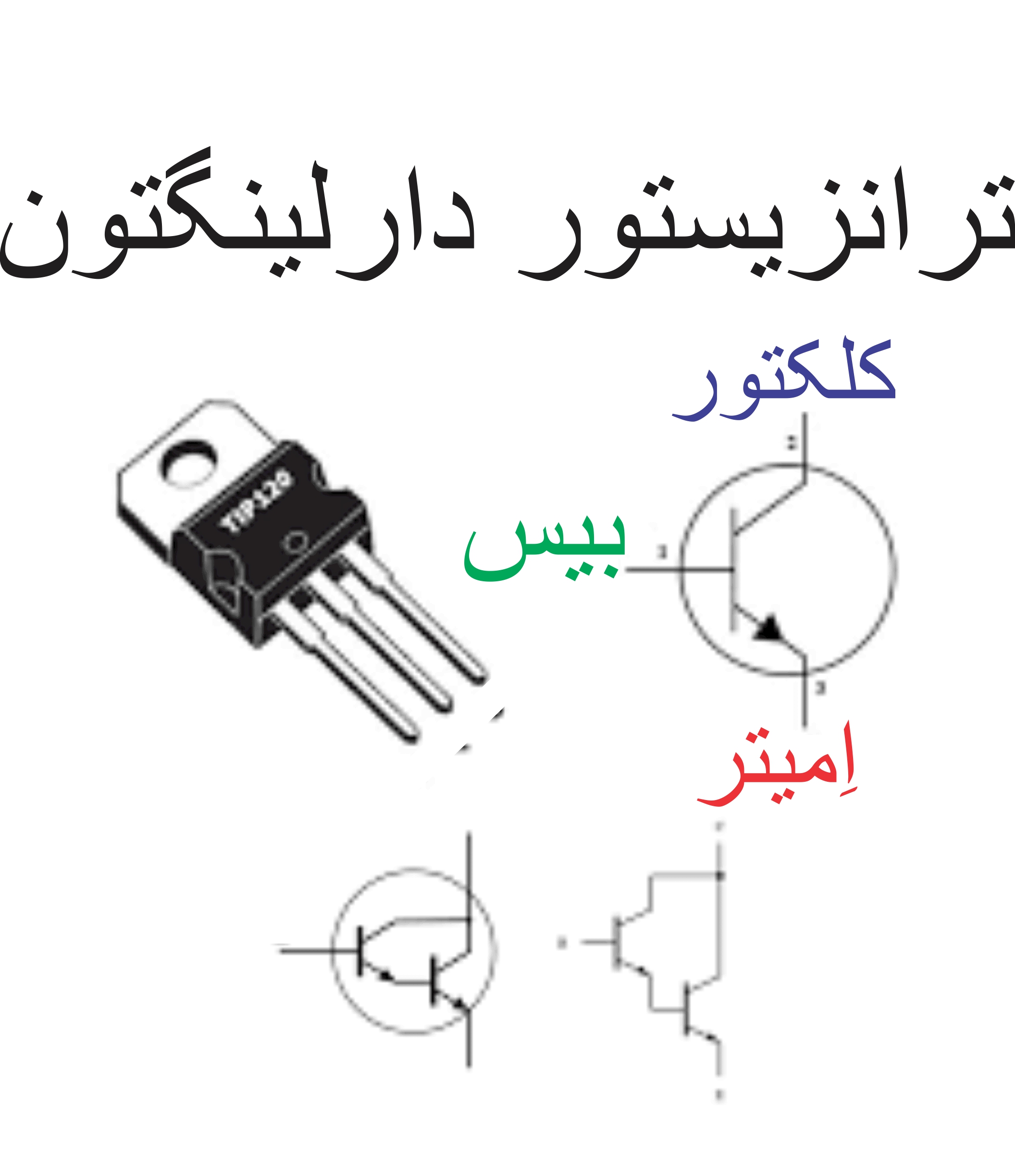
Structurally, a Darlington transistor can be modeled as two transistors.
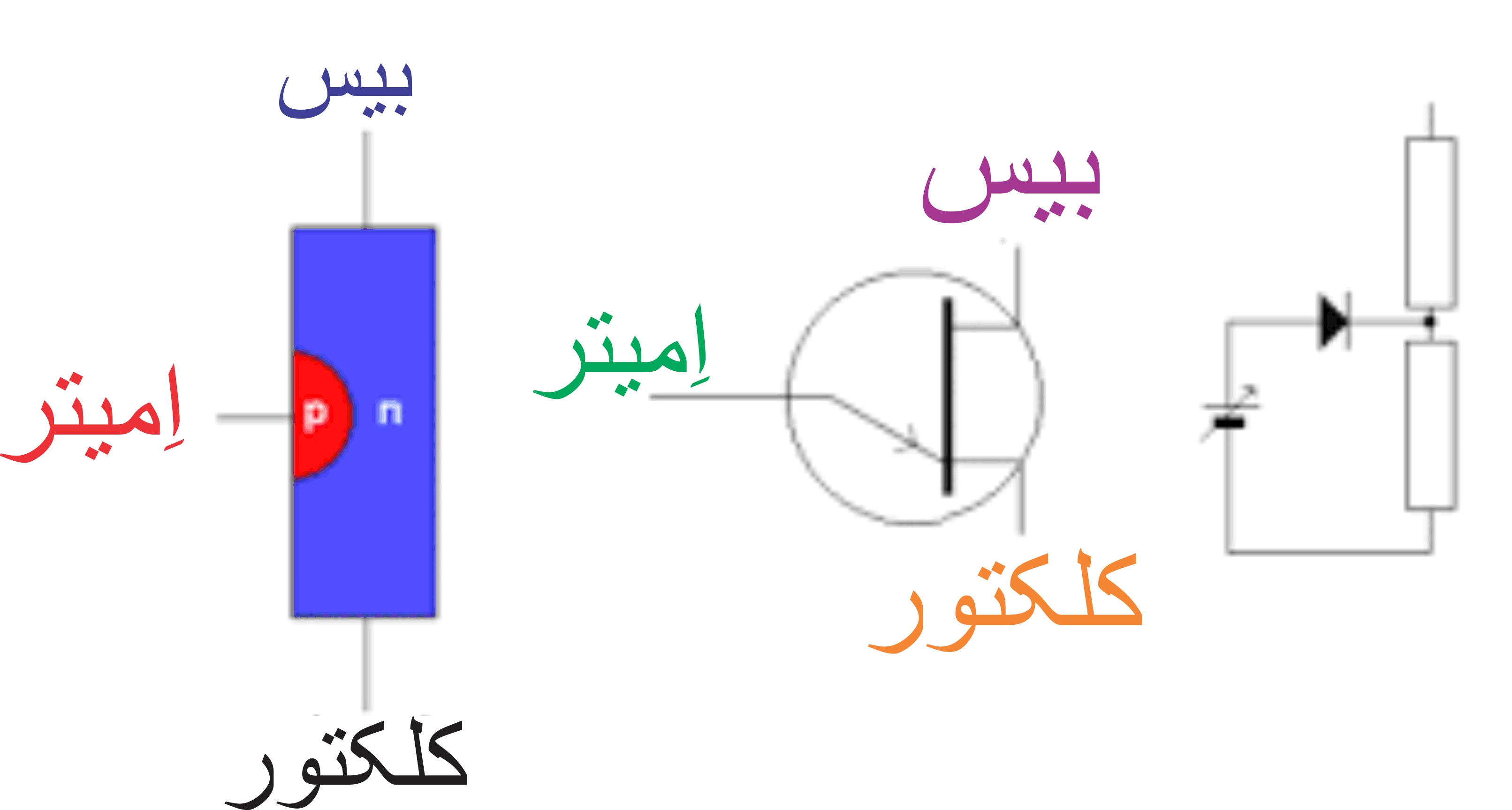
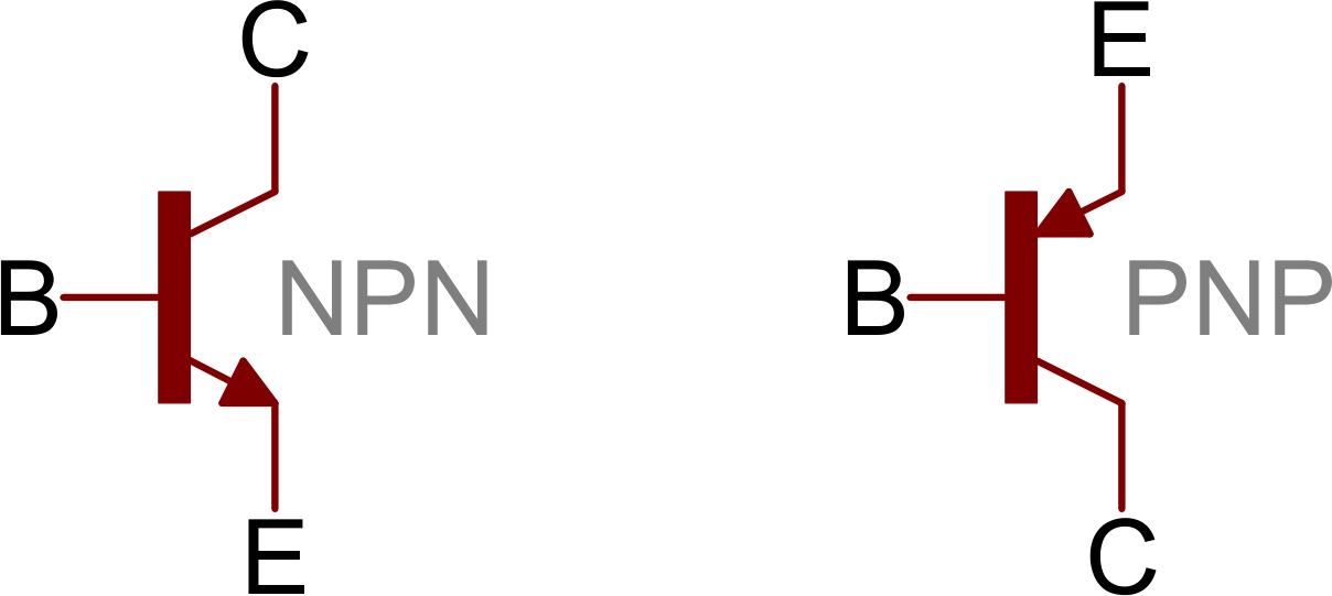
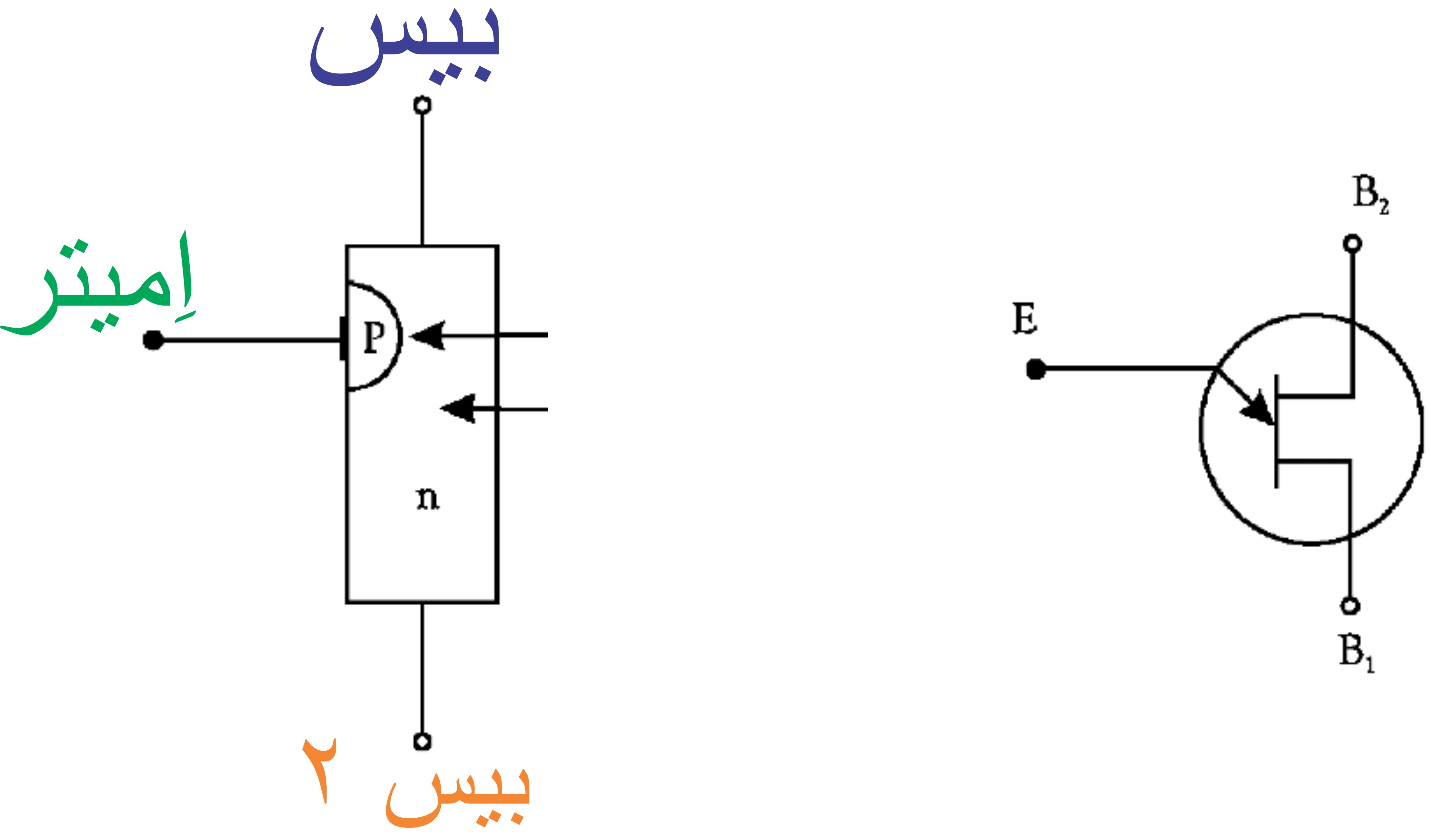
The basic Darlington transistor consists of two semiconductor junctions and can be divided into two main types, PNP or NPN, depending on how these junctions are connected to each other. To understand how a transistor works, we first need to understand how a semiconductor junction works. You see a PN junction. It is made by connecting two pieces of P and N semiconductors together. N-type semiconductors have free electrons and P-type semiconductors have a large number of free holes. Simply put, a free hole is a space where there is a shortage of electrons.
Reverse bias in Darlington transistors
If we apply a voltage to this piece of semiconductor from the outside, a current will flow in the circuit, and if we change the direction of the applied voltage, no current will flow through the circuit. This semiconductor junction models the simple operation of a diode. One of the applications of a diode is to rectify alternating currents. Since a capacitor is usually formed at the junction of an N-type semiconductor to a P-type semiconductor, the frequency response of a PN junction depends entirely on the quality of construction and the size of the junction capacitor. For this reason, the first Darlington transistors built were not capable of operating at radio frequencies - for example, for detection.Usually, to reduce this unwanted capacitance, the junction area is reduced and brought to a single point.

Effect of voltage on emitter and collector terminals in Darlington transistors
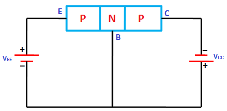
For each of the semiconductor layers in a Darlington transistor, a base is provided that allows the external circuit to connect to the semiconductors. These bases are known as Base, Collector, and Emitter. If we look at the layer structure of a transistor, it seems that there is no particular difference between Collector and Emitter, but this is not the case. Because the thickness and size of the Collector layer is much larger than the Emitter layer, and this practically makes these two layers different from each other despite their similar polarity. The working principle of the Darlington transistor is as follows: if we directly bias the BE junction (Bias means applying voltage and excitation) so that this PN junction turns on (for this, it is enough to apply a voltage of about 0.6 to 0.7 volts to this junction, depending on the type of transistor), then a very high current can be drawn from the closed circuit between the emitter and the collector. In the normal case, there is no gap circuit between the emitter and the collector.
Researcher and author: Dr. ( Afshin Rashid)
Specialized PhD in Nano-Microelectronics