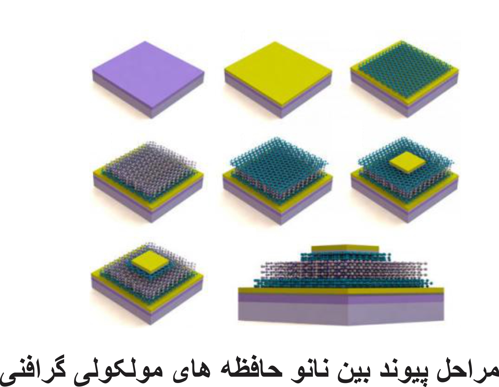
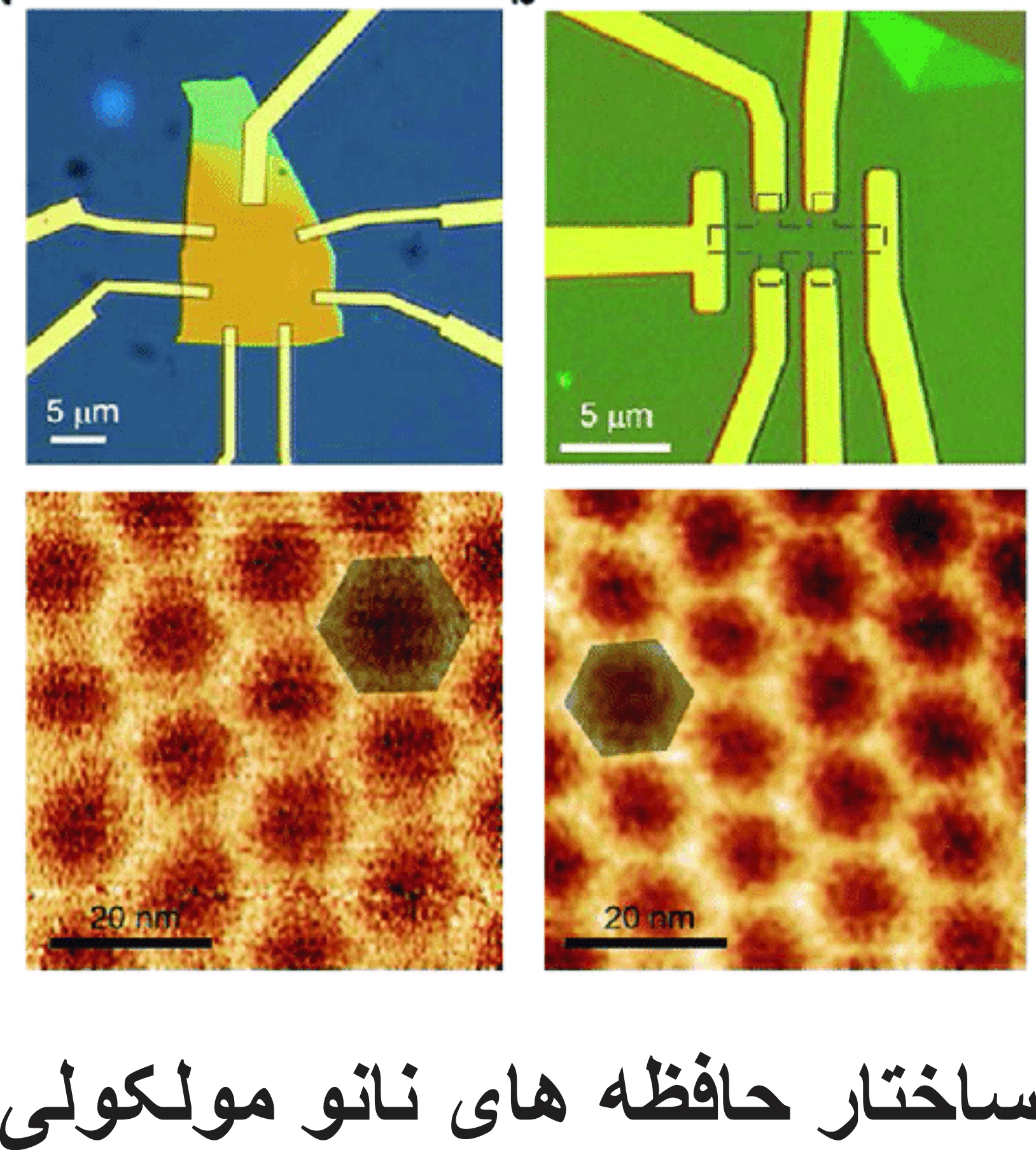
Testing the link between Nano Memory Moulcolar graphene molecular nano memories and graphene nano transistors to reproduce and produce this type of electrical nano memory.
Researcher and author: Dr. ( Afshin Rashid)
Note: Graphene, which consists of only one carbon atom, can be used to create multi-layer graphene molecular nano memories that consume less energy and occupy little space. Graphene is a semi-conducting material with zero gap and not suitable for logic circuits, but using nano technology, they create different forms of this material that have different gaps.
Graphene nanoribbons, multilayer graphene and graphene grown on Si are such forms. The term "nano-transistor" comes from the combination of the word "nano-scale" in transmission and resistance. In a Si graphene field effect nano transistor, the resistance between two electrodes can be transferred or controlled by a third electrode. In a Si multilayer graphene field effect nano transistor, the current between the two electrodes is controlled by the electric field from the third electrode. Unlike the bipolar transistor, it is capacitively connected to the third electrode and is not in contact with the semiconductor. Three electrodes are connected to the source, drain and gate in the structure and internal structure of multilayer graphene molecular nano memories .
By using the structure of nanomolecular memory , the size of the memory bits can be basically reduced, thereby increasing the density of the magnetic memory and its efficiency, and lowering its cost. Nano lithography methods are now being used to prepare some very powerful memories. The science and technology of nanoelectronics provide different possibilities of nano molecular memory . For example, photorefractory materials represent only one type of optical memory. In fact, by using nano technology, the storage capacity of information can be increased by a thousand times or more. Storing subject information is very important and necessary, which can be done in different ways through nanomolecular memories .The role of graphene nanosheets (GA) in the construction of nanotransistor (Nano Transistor) in the form of an electric field created by the gate electrode controls the current created by the source and drain electrodes. Drain current transport is modulated by changing the density of charge carriers in the two-dimensional transport channel. In the multilayer Si graphene field effect nanotransistor, a 3D transmission channel, the drain current is modulated by the thickness of the 3D transmission channel. In the circuit diagram of a multilayer GA graphene field effect nanotransistor, the source and drain electrodes are directly connected to the semiconductor. While the gate electrode is capacitively connected to the semiconductor using gate dielectric. Many chemical and physical methods have been proposed to produce different types of multilayered nanographene.
Conclusion :
Graphene, which consists of only one carbon atom, can be used to create multi-layer graphene molecular nano-memories that consume less energy and occupy little space. Graphene is a semi-conducting material with zero gap and not suitable for logic circuits, but using nano technology, they create different forms of this material that have different gaps.
Researcher and author: Dr. ( Afshin Rashid)
Specialized doctorate in nano-microelectronics


