

Section _ Construction and formation of field effect transistors (Mosfet)
(Depletion channel) and (Formation channel) in a field effect transistor (Mosfet)
Researcher and author: Dr. ( Afshin Rashid)
Note: The most common and important electronic component in electronic and power circuits is the transistor; MOSFET field effect transistors are made in two ways.
Depletion-mode MOSFETs (DMOSFET) and Depletion-mode MOSFETs (EMOSFET) Enhancement-mode MOSFETs (EMOSFET) and EMOSFETs Each of these two types of transistors can be made with either an n-channel or a p-channel. The most common MOSFETs on the market are the n-channel MOSFETs, which are depletion-type, and the p-channel MOSFETs, which are enhancement-type. The most famous field-effect transistor in analog and digital electronic circuits is the MOSFET. The term "metal-oxide" should not be mistaken for "metal oxide". The reason for this name is that in the structure of this transistor, a layer of silicon oxide (SiO 2 ) is placed under the metal connection of the gate base.
Internal structure and types of MOSFET field effect transistors
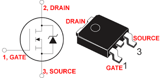
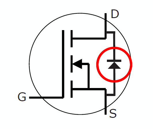
A MOSFET consists of a gate (G), drain (D), source (S), and body (B) terminals. The body (B) is often connected to the source; therefore, a MOSFET has three terminals. A field effect transistor (FET) is considered to have three terminals, namely, Gate, Drain, and Source. In this transistor, the gate (control terminal) does not conduct current, and as the name suggests, the current through the FET is controlled only by applying a voltage and creating an electric field within the semiconductor.
MOSFET transistor with N-type depletion semiconductor channel:
This type of transistor consists of a p-type element with low impurity. Inside this element, two n-type bases with high impurity are created. These regions are connected to each other by a n-type channel region with low impurity. From the sides of the channel, drain-source contacts come out. The gate is made of metal, which is separated by a layer of silicon dioxide. This type of MOSFET is called a completely closed channel (DMOSFET).

In most MOSFETs, the base crystal is internally connected to the source, but in some cases a fourth junction may be brought out of it. In such cases, this junction must be connected to the source base in order for the base and channel np junction to always remain in reverse bias.
Enhancement MOSFET (EMOSFET) structure
In this type of transistor, unlike the depletion-channel transistor, the channel is not created during manufacturing. Therefore, until the gate of the transistor is biased, the transistor remains off. Due to the very high resistance of the base crystal that separates the drain and source from each other from increasing with VDS, a noticeable current does not pass through the drain and practically does not pass through it.

If we bias the gate-source so that the gate potential is more positive than the source, the electrostatic field of the gate attracts a number of free electrons from the +n regions and the base crystal and creates a narrow channel inductively between the drain and source . This channel reduces the resistance between the two bases and causes a current (drain).
Researcher and Author: Dr. ( Afshin Rashid)
Specialized PhD in Nano-Microelectronics