Field Effect Nano Transistors (Nano Teransistor Mosfet)
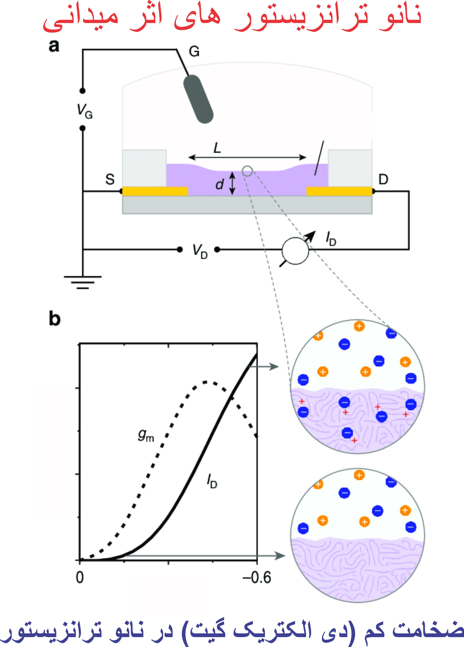
bulk MOSFET field effect nanotransistors ( low gate dielectric thickness in nanotransistors)
Researcher and author: Dr. ( Afshin Rashid)
Note: in the structure of field effect nano transistors based on carbon nanotubes - graphene with bulk MOSFET of the upper gate for more gain, the carbon nanotubes are completely placed inside the gate insulation. Unlike carbon nanotube field effect transistors Back gate, it is possible to make a large number of this type of tube nano transistor on a wafer, because the gates of each one are separate.
Also, due to the small thickness of the gate dielectric in the nano-transistor, a larger electric field can be created with a low voltage on the carbon nano-tube. Although the manufacturing process is more complicated than back-gate carbon nanotube field-effect transistors, the above advantages make this type preferable. In the structure of field effect nanotransistors based on carbon-graphene nanotubes with bulk MOSFET , all nanotransistors on a wafer are turned off and on at the same time, because they have the same gate. It is such that the contact surface of the carbon nano tube with the gate oxide is small and it creates a problem to turn the part on and off with low voltage.
For the production of nanotransistors and nanochips, one of the advantages of these methods is the ease of changing the process parameters and achieving optimal conditions for the production of carbon nanotubes. A major challenge in the fabrication of field-effect nanotransistors based on carbon-graphene nanotubes with bulk MOSFETs is the impurities in the products. Placing the gate around and in the entire nanotube that improves the performance. First, the carbon nanotube that has an insulating coating is placed on the wafer, and the source and drain metal connections are placed on both sides of it, then to determine To separate the source and drain area, si is added under the carbon nanotube. This removal continues until reaching the insulation of the substrate. Then, by using materials that have a high dielectric coefficient, insulation is created between the gate and the source and the drain, as well as metal on this insulation to better connect the metal of the gate to the Graphene-carbon nanotubes are placed with bulk MOSFET.
Conclusion :
In the structure of field effect nano transistors based on carbon nanotubes - graphene with bulk MOSFET of the upper gate for more gain, the carbon nanotubes are completely placed inside the gate insulation. Unlike back gate carbon nanotube field effect transistors , it is possible to make a large number of this type of tube nano-transistor on a wafer, because the gates of each one are separate.


