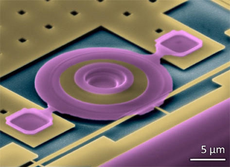
Electron beam nano-lithography (below 100 nm _ range 10 nm ) in the manufacture of graphene nano-transistors (PhD nano-microelectronics)
Researcher and author: Dr. ( Afshin Rashid)
Note: Similarly , electron beam nano-lithography , in the case of nano-processes, relies on changing the solubility of the resistor after exposure. However, in electron beam nano-lithography, electron-sensitive resistance should be used instead of the image capture.
Electron beam nano-lithography is usually performed in a special environment or in equipment specially designed for this purpose. In both cases, an electron beam with accurate focus is scanned sequentially along the sample to show resistance. The electron beam nano-lithography process is inherently slow compared to other methods because the electron beam requires a limited time at each point of exposure. It is rare to be exposed to a sample multiple times. Some developments are underway for multi-electron beam exposure . In contrast to long exposure times, very high resolution (below 100 nm) is typically achieved by electron beam nano-lithography and, with a little optimization and appropriate equipment, reaches the range of 10 nm, as in Electron beam nano-lithography occurs, positive and negative resistances are present in electron beam nano-lithography as well as the ability to perform lifting processes that save the etching stage. Electron beam nano-lithography is a good technique for laboratory research and prototyping, given that throughput is not an important issue and a very good solution is obtained.
Graphene has special electrical properties that make it a promising candidate for future nanoelectronics. While graphene, a single-dimensional carbon layer, is a conductive material, it can be converted into a semiconductor as a nanowire. This means that it has enough energy or a band gap in which there is no electron mode - it can be turned on and off, and therefore may become a major component of nanotransistors. The role of graphene nano-plates (GA) in the fabrication of nano transistors The electric field generated by the gate electrode controls the current generated by the two source and drain electrodes. The drain current is modulated by changing the density of the charge carriers in the two-dimensional transmission channel. In the nanotransistor, the effect of a multi-layer Si graphene field is modulated by a three-dimensional transmission channel with a three-dimensional transmission channel thickness . In a circuit diagram of a multilayer GA graphene field nanotransistor, two source and drain electrodes are connected directly to the semiconductor, while the gate electrode is capacitively connected to the semiconductor using a gate dielectric.
Conclusion :
Similarly , electron beam nano-lithography , in the case of nano-processes, relies on changing the solubility of the resistor after exposure. However, in electron beam nano-lithography, electron-sensitive resistance should be used instead of the image capture.
Researcher and author: Dr. ( Afshin Rashid)
PhD in Nano-Microelectronics


