Interfering Nano-Lithography (IL) and Nano-Optoelectronics (PhD in Nano-Microelectronics)
Researcher and author: Dr. ( Afshin Rashid)
Note: The ability to produce large microstructures and nanostructures on non-flat surfaces is important for many applications such as optics, optoelectronics, nano-photonics, imaging technology, NEMS and microfluids.
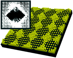
However, it is very difficult to create large nanostructures on curved or non-planar surfaces using existing modeling methods. In addition, the current types of nanotechnology technologies such as electron beam lithography (ELB), optical lithography, interference lithography (IL), etc., can not meet all the application demands of industrial applications in terms of high resolution, high power, low cost. . , Large area and olgoes on uneven and curved surface. Therefore, new high-volume nanotechnology technology is in dire need of exploitation and development to meet the tremendous needs of emerging markets.Nanoelectronic lithography is currently considered as a promising low-cost, high-power, high-resolution nano-pattern method, especially for the production of small-scale / large-scale nano-patterns and complex 3D structures. The above aspects have also created proportional features due to these salient advantages. The conversion of optical structures in combination with the construction of a large area becomes a more effective method in this field. In particular, nanoelectronic lithography has great potential for setting new benchmarks for the construction of miniature, low-cost, low-weight optics that can be used in many applications.
To better understand the relationship between the optical, electronic, magnetic and catalytic properties of nanoparticles and their structure, well-defined model systems are needed. Chemical synthesis of metal nanoparticles leads to large size and shape scattering and lateral irregularities. In contrast, conventional top-down lithographic techniques provide control of lateral order and dimensions. However, they are either limited in resolution or have little power, and therefore do not activate the large patterning area required to obtain the appropriate signal-to-noise ratio in conventional analytical and descriptive techniques. Intense ultraviolet (EUV) lithography has the advantages of efficiency and simplicity of photolithography as well as high resolution due to wavelength.
Conclusion :
The ability to produce microstructures and nanostructures on non-planar surfaces is important for many applications such as optics, optoelectronics, nanophotonics, imaging technology, NEMS and microfluids.
Researcher and author: Dr. ( Afshin Rashid)
PhD in Nano-Microelectronics


