

Field Effect Nano Transistors (Nano Teransistor Mosfet)
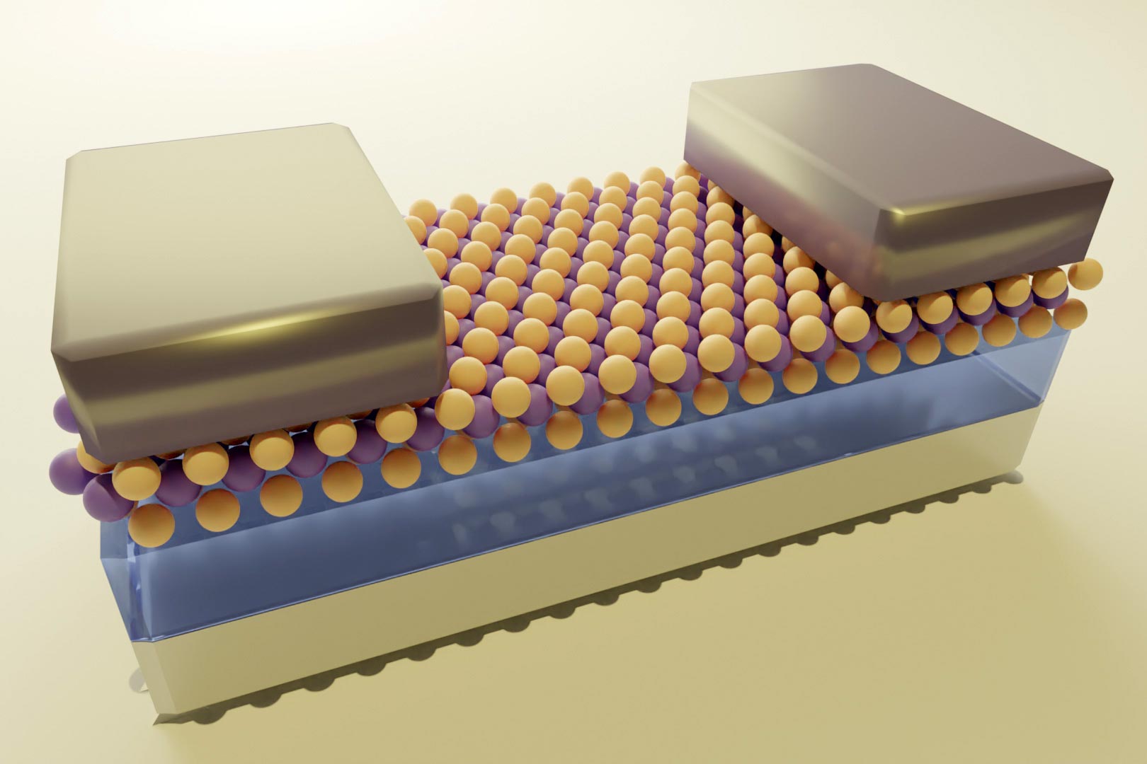
A graphene field effect nanotransistor (multilayer Si) ( nanotransistor with multilayer graphene and grown graphene)
Researcher and author: Dr. ( Afshin Rashid)
Note: The term "nano-transistor" comes from the combination of "nano-scale" in transmission and resistance. Nanographene is a semi-conducting material with zero gap and not suitable for logic circuits, but using nano technology, they create different forms of this material that have different gaps. Graphene nanoribbons, multilayer graphene and graphene grown on Si are such forms.
In a Si graphene field effect nano transistor, the resistance between two electrodes can be transferred or controlled by a third electrode. In a Si multilayer graphene field effect nano transistor, the current between the two electrodes is controlled by the electric field from the third electrode. Unlike the bipolar transistor, it is capacitively connected to the third electrode and is not in contact with the semiconductor. Three electrodes are connected to the source, drain and gate in the Si multi-layer graphene field effect nano transistor structure.
In the circuit diagram of a multilayer Si graphene field effect nanotransistor, the source and drain electrodes are directly connected to the semiconductor, while the gate electrode is capacitively connected to the semiconductor using a gate dielectric. The electric field created by the gate electrode controls the current created by the source and drain electrodes. Drain current transport is modulated by changing the density of charge carriers in the two-dimensional transport channel. In the multi-layer Si graphene field effect nano transistor, a 3D drain current transmission channel is modulated by the thickness of the 3D transmission channel. Many chemical and physical methods have been proposed to produce different types of multilayered nanographene. The basis of the work of physical methods is that in these methods, the forces between the graphene sheets are tried remove the graphite and separate them to reach single layers of graphene or graphene oxide, which is the same top -down method. In chemical methods, multi-layered nanographene is made by placing individual carbon atoms together, which is also called the bottom-up method.

Conclusion :
The term "nano-transistor" comes from the combination of the word "nano-scale" in transmission and resistance. Nanographene is a semi-conducting material with zero gap and not suitable for logic circuits, but using nano technology, they create different forms of this material that have different gaps. Graphene nanoribbons, multilayer graphene and graphene grown on Si are such forms.
Researcher and author: Dr. ( Afshin Rashid)
Specialized doctorate in nano-microelectronics