

Field Effect Nano Transistors (Nano Teransistor Mosfet)
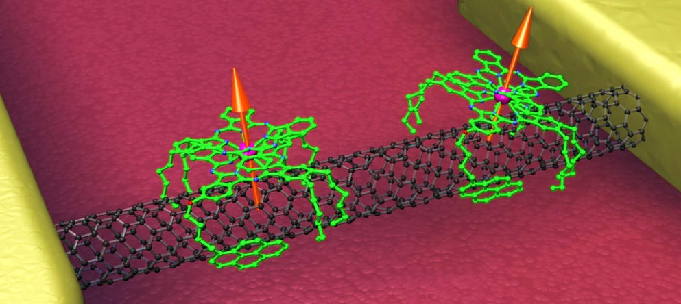
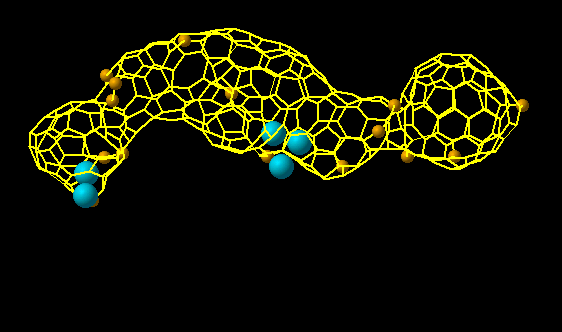
Field effect nanotransistors based on (carbon nanotubes)
Researcher and author: Dr. ( Afshin Rashid)
Note: All field nano transistors on a wafer are turned off and on at the same time because they have the same gate. The thickness of the oxide layer is large, and on the other hand, the production process is such that the contact surface of the carbon nano tube with the gate oxide is small and for turning off and on Making the part with low voltage creates problems.
In the structure (field nano transistors) of the upper gate , carbon nanotubes are placed completely inside the gate insulation for greater gain. Unlike the back gate carbon nanotube field effect transistors, a large number of this type of transistor can be placed on He made a wafer, because the gates of each one are separate. Also, due to the small thickness of the gate dielectric in the nano-field transistor, a larger electric field can be created with a low voltage on the carbon nanotube. Although the manufacturing process is more complicated than back-gate carbon nanotube field-effect transistors, the above advantages make this type preferable.
Internal structure of field effect nano transistors based on (carbon nanotubes)
Irregular nanotubes may cause a short circuit between output and feed. The connection between carbon nanotubes and metal, which is used to connect the source and drain, forms a Schottky barrier (SB) in a field-effect nanotransistor based on (carbon nanotubes) . The formation of Schottky barriers in the source and drain of a transistor causes a significant reduction in the current sent in the transistor. Therefore, for the higher operational efficiency of the field-effect nanotransistor parts (carbon nanotubes) , suitable metals are needed that can be used at the junction of the drain and the drain and create an ohmic connection.
Electric field of field effect nano transistors based on (carbon nanotubes)
When an electric field is applied to field effect nano transistors based on (carbon nanotubes) , the carbon nanotube that is between the source and the drain contains the moving charge. The density of these charges is for the source and this density is given by (Drain) the probability of the Dirac Fermi distribution is determined. The ability of carbon nanotubes to be used in gas sensors is due to their hollowness and high contact surface. This contact surface consists of the outer wall of the nanotube and its empty middle parts. Physico-chemical absorption of gases in nanotubes changes their conductivity.
Researcher and author: Dr. ( Afshin Rashid)
Specialized doctorate in nano-microelectronics