

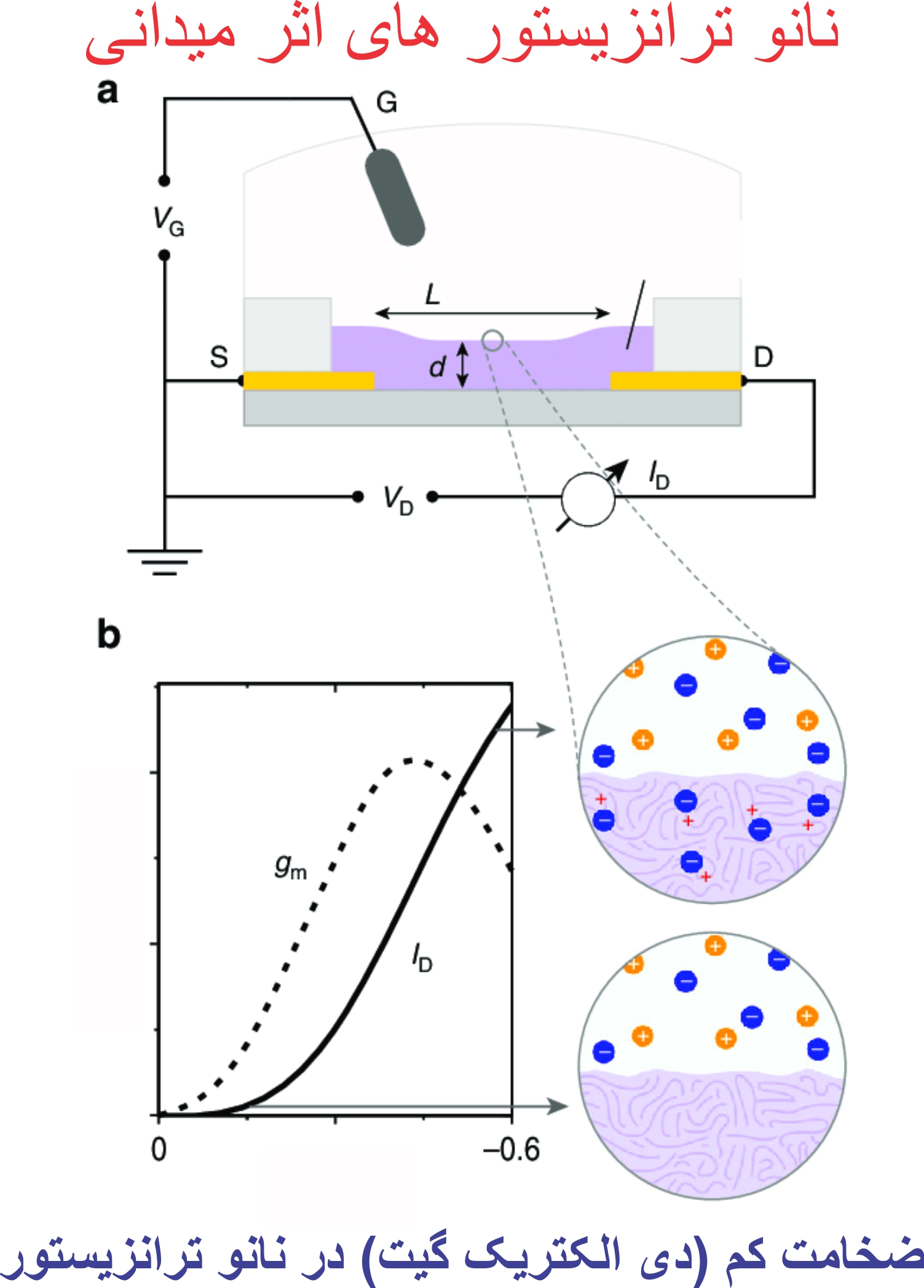
Field Effect Nano Transistors (Nano Teransistor Mosfet)
Pattern miniaturization techniques in the design of nanodevices such as field effect nanotransistors
Researcher and author: Dr. ( Afshin Rashid)

Note: Micro/nano patterning is a pattern miniaturization technique, especially for electronics. Today, using soft lithography has become a standard in biomaterials engineering and fundamental research in cell biology. It generally uses lithographic methods, but many techniques have been developed. Batch fabrication of microstructures requires a low-cost, high-throughput surface pattern.
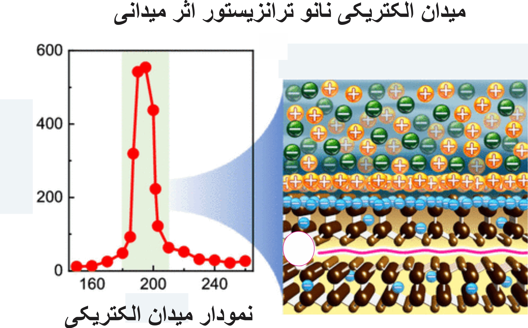
Micro/nano patterning is one of the pattern miniaturization techniques in the design of nanodevices such as nanotransistors and nanodiodes, nanoswitches and nanological gates, in order to design nanoscale computers with dual scale capabilities. All living biological systems function due to the molecular interactions of various subsystems. Molecular building blocks (proteins and nucleic acids, lipids and carbohydrates, DNA and RNA) can be used as an inspiring strategy on how to design high-performance NEMS and MEMS that have the required characteristics and properties. commented In addition, analytical and numerical methods are available to analyze the dynamics and three-dimensional geometry, bonding, and other properties of atoms and molecules. Therefore, electromagnetic and mechanical, and other physical and chemical properties can be studied. Nanostructures and nanosystems can be widely used in medicine and health. Among the possible applications of nanotechnology, the following can be mentioned: drug synthesis and drug delivery (therapeutic potential is greatly increased due to the effective direct delivery of new types of drugs to specific locations in the body), nanosurgery and nanotherapy. , genome synthesis and detection, nanoscale stimuli and sensors (diagnosis and prevention of disease), design and implantation of irrefutable artificial organs, and design of high-performance nanomaterials. It is important that these technologies change the construction and production of materials, devices and systems.

Nanolithography is a branch of nanotechnology that deals with the study and application of nanostructures of nanoscale structures, meaning nanopatterns with at least one lateral dimension between the size of an individual atom and approximately 100 nm , but today whenever this If the term is related to nanotechnology, we understand something different. Nanolithography is used, for example, when nanofabricating advanced semiconductor integrated circuits (nanocircuits), for nanoelectromechanical systems (NEMS), or for almost any other fundamental application in various scientific fields in the field of nanosearch. This technology can be suitable for the production of nano-type semiconductor integrated circuits (IC), NEMS and for various applications in research. It is also possible to modify semiconductor chips on the nano scale (in the range of 9-10 m).

Conclusion :
Micro/nano patterning is one of the pattern miniaturization techniques, especially for electronic devices. Today, using soft lithography has become a standard in biomaterials engineering and fundamental research in cell biology. It generally uses lithographic methods, but many techniques have been developed. Batch fabrication of microstructures requires a low-cost, high-throughput surface pattern.
Researcher and author: Dr. ( Afshin Rashid)
Specialized doctorate in nano-microelectronics