

بخش _ بررسی سیستم و اَدوات نانو اِلکترونیک
شناخت و تشریح نانو سیستم های چند منظوره MEMS و مدارهای مجتمع میکروالکترونیک
پژوهشگر و نویسنده: دکتر( افشین رشید )
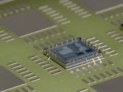
نکته: میکرو الکترومکانیکال سیـستم هـا (MEMS) ،مجتمـع سازی عناصـر مکـانیکی ، سنـسور ها، محرکها و ادوات الکترونیک روی پایـه سـیلیکونی بوسـیله تکنولـوژی ساخت در حد ابعاد میکرون اسـت، مادامیکـه ادوات الکترونیک برای استفاده در رشـته فرآینـد مـدارهای مجتمع ( IC) سـاخته مـی شـوند ( ماننـد فرآینـد اجـزاء ) ، " BICMOS ، Bipolar ، CMOS سـاختن میکرو مکانیکال " برای استفاده در فرآیند های میکروماشین کردن سـازگار و مناسـب بـا آن کـه بـه طـور انتخابی قسمت به قسمت با قرص های سیلیکونی یـا افزودن لایه های ساختمانی جدید بـرای شـکل دادن ادوات مکانیکال و الکترومکانیکال استفاده مـی شـود، ساخته می شوند .
MEMS نویـد انقلابـی نـوین را در زمینـه محـصولات مجتمـع ســازی ســیلیکون کــه بــر پایـه تکنولـوژی میکرو الکترونیک و میکرو ماشین ها نباشد، میدهد کـه در جهت ممکن ساختن تحقق کامل " سیستم ها دریک تراشه " ا ست . MEMS یک فناوری است که اجازه توسعه محصولات هوشمند ، تکمیل توانایی محاسباتی میکرو الکترونها با در نظـــر گـــرفتن قابلیتهـــای میکرو سنـــسور ها و میکرو محرکهـا و توســعه فــضای ممکـن طراحــی و استفاده را می دهد . مدارهای مجتمع میکرو الکترونیک می تواند به عنـوان مغز متفکر یک سیستم در نظر گرفته شود و MEMS این قابلیت تصمیم گیری را با چـشم هـا و بازوهـایی زیاد کرده تا به میکرو سیستم ها اجازه دهد تا محیط به وسیله اندازه گیری مکانیکی ، دمایی ، بیولوژیکی شیمیایی ، نوری و مغناطیسی جمع آوری می کننـد. الکترونیک سپس اطلاعات گرفته شده از حـسگرها و از طریق بعضی تصمیم گیریها به بازوها برای واکـنش نشان دادن به وسیله حرکت کردن ، تثبیت موقعییت، تنظیم کردن ، پمپ کردن و فیلتر کردن دستور میدهد. در نتیجه کنتـرل محـیط بـرای خواسـته هـای مطلوب انجام می شود. برای اینکه ادوات MEMS برای استفاده در شیوه های ساخت گروهی مانند مـدار های مجتمـع سـاخته مـی شـوند ، سـطوح جدیـدی از قابلیـت انجـام وظیفـه ،قابلیت اطمینان و مهارت می توانـد روی یـک تراشـه سیلیکونی کوچک با یک هزینـه نـسبتا "پـایین قابـل دسترسی باشد.

فرآیند های ترکیـب ،طراحی و بهینه سازی در واقع تکاملی بر نمونه هـای طبیعی هستند . در هـر ســطح از سلـسله مراتـب طراحــی ، کــارآیی سیستم در قلمرو رفتار آن برای ارزیابی ،بهینه سـازی و تصحیح فرآیند بهیینه سازی و ترکیب استفاده مـی شود تا راه حل های جدیـد پیـدا شـود . IC هـا بایـد مشخصه های عملکرد MEMS مانند کنتـرل ادوات و ســاختار های الکترومکــانیکی مبتنــی بــر الکتــرومغناطیس ، کانالهـای ورودی - خروجـی ، تبـدیلات آنالوگ به دیجیتـال و دیجیتـال بـه آنـالوگ ، فیلتـر کردن ، استفاده از داده ها و غیره را تـضمین کننـد.MEMS بـی نهایـت کوچکنـد. موتـور هـای متحـرک کوچکتر از قطر مو، در عین حال تکنولـوژی MEMS اصولا "در باره انـدازه هـا بحـث نمـی کنـد . MEMS معمولا "به وسیله تکنوژی سیلیکونی ساخته می شود. زیرا سیلیکون دارای خواص خوبی است که آن را به یک انتخاب عالی برای کاربرد هـای مکـانیکی سـطح بالا تبدیل کرده است ، برای مثال نسبت استحکام به وزن سـیلیکون از بـسیاری از مـوارد مهندسـی دیگـر بالاتر است که این خاصـیت دسـت یـافتن بـه ادوات مکانیکی دارای پهنای باند زیاد را ممکن می کند.

نتیجه گیری :
نو آوری و دور اندیشی عمیـق MEMS یـک تکنولوژی ساخت جدید است و راهـی بـرای سـاختن سیستم های الکترومکـانیکی پیچیـده کـه در تکنیـک های ساخت مجتمع استفاده می شود ، همانند آنچـه که برای مدارهای مجتمع (IC) استفاده می شود و در انتها جمع آوری این عناصر الکترومکانیکی بـه کمـک علم نانو _ میکرو الکترونیک ممکن میباشد .
پژوهشگر و نویسنده: دکتر ( افشین رشید)
دکترایِ تخصصی نانو _ میکرو الکترونیک