

The Role of Graphene Nano Sheets (GA) in the Construction of Nano Transistors Based on PhD Nano-Microelectronics
Researcher and author: Dr. ( Afshin Rashid)
Note: The role of graphene nanoplate (GA) in the construction of nano transistors as an electric field created by the gate electrode controls the current created by the two electrodes source and drain. The drain current is modulated by changing the density of the charge carriers in the two-dimensional transmission channel. In the nanotransistor, the effect of a multi-layer Si graphene field is modulated by a 3D transmission current channel with a three-dimensional transmission channel thickness.
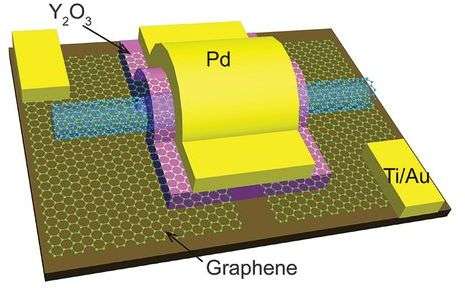
In the circuit diagram of a multilayer GA graphene field nanotransistor, two source and drain electrodes are connected directly to the semiconductor, while the gate electrode is capacitively connected to the semiconductor using a gate dielectric. Numerous chemical and physical methods have been proposed for the production of various types of multilayer nano-graphene. The basis of physical methods is that in these methods, they try to eliminate the forces between the graphene plates in graphite and by separating them, they reach the graphene or graphene oxide monolayers, which is the same method top- down. Is. In chemical methods, multilayer nano-graphene is made by putting together individual carbon atoms, which is also called the bottom-up method.
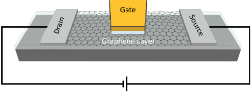
Graphene, which consists of only one carbon atom, can be used to create multilayer graphene field effect nanotransistors that consume less energy and take up less space. Graphene is a semiconductor material with zero gap and unsuitable for logic circuits, but using nanotechnology, they create different forms of this material that have different gaps. Graphene nano-strips, multilayer graphene and graphene grown in the structure of nanotransistors are such forms. The term nano-transistor comes from the combination of the term nano-scale in transmission and resistance. In a graphene Si field effect nanotransistor the resistance between two electrodes can be transmitted or controlled by a third electrode. In a multilayer graphene field effect nanotransistor, the current between the two electrodes is controlled by an electric field from the third electrode.

Conclusion :
In the circuit diagram of a multilayer GA graphene field nanotransistor, the two source and drain electrodes are connected directly to the semiconductor, while the gate electrode is capacitively connected to the semiconductor using a gate dielectric. Numerous chemical and physical methods have been proposed for the production of various types of multilayer nano-graphene transistors.
Researcher and author: Dr. ( Afshin Rashid)
PhD in Nano-Microelectronics