The synthesis of nano-crystals by physical vapor deposition (PVD) PhD in microelectronics, nano _
Researcher and author: Dr. ( Afshin Rashid)
Note: physical vapor deposition (PVD) one of vacuum deposition methods that can be used to produce thin films and coatings used. Physical vapor accumulation, or PVD for short, is the process by which a substance is converted from a solid or liquid phase to a vapor phase and then accumulates again as a thin layer in a solid or liquid phase on the surface. Spraying and evaporation are the most common processes of physical accumulation of steam. PVD is used to make components that require thin films with specific functions including mechanical, optical, chemical, and electronic properties.
In the process of dealing PVD floating ions in the plasma levels of early accumulation of atoms on the surface and dug it sits on the surface of the base material and a thin layer on the surface can be. Nanocrystals are substances whose constituent particles are arranged in three regular directions. If the atoms or ions manufacturer regular way to learn something crystal is (ie a periodic arrangement of atoms in the crystal due to three dimensions, internal order). Crystals characterized by well-developed crystalline faces (external surfaces) are described as .
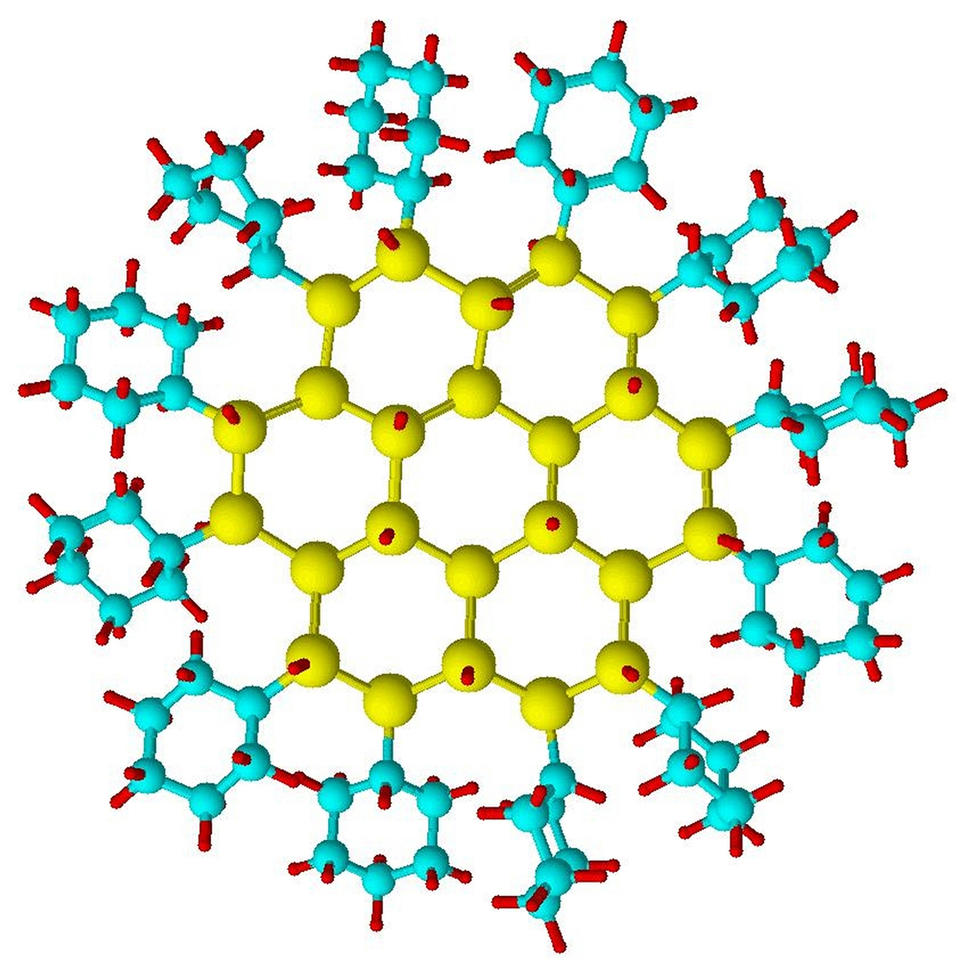
A crystal is made by arranging atoms and groups of atoms in regular patterns, for example at the corners of a cube or rectangle prism . The basic arrangement of the atoms that describes the crystal structure is determined. This cell is called a unit. The crystals must have a balanced charge . This means that the amount of negative charge must be compensated with the same amount of positive charge. A nanocrystal is a material particle having at least one dimension smaller than 100 nanometers, based on quantum dots . (A nanoparticle ) and consists of atoms arranged in either single or polycrystalline . The size of the nanocrystals distinguishes them from larger crystals .For example, silicon nanocrystals can emit efficient light, while bulk silicon does not and can be used for memory components. When embedded in solids, nanocrystals may exhibit much more complex melting behavior than conventional solids and may form the basis of a particular class of solids. They can act as single-domain systems (intra-system volumes with the same atomic or molecular arrangement) that can help explain the behavior of macroscopic specimens of the same material without the complexity and similarity of other particles . Semiconductor nano-crystals with dimensions less than 10 nm as well as quantum dots are described .Crystals whose refractive index is the same in all three crystal directions are called isotropic crystals. In contrast, crystals that have different refractive index in one, two or three directions are called anisotropic crystals. Nanoscale crystals, which are cut very frequently, are powerful catalysts for chemical reactions. And the unusual shape of the crystals causes the atoms of the nanocrystals to align themselves in an uneven way to increase reactivity.
Conclusion :
Physical vapor deposition (PVD) one of vacuum deposition methods that can be used to produce thin films and coatings used. Physical vapor accumulation, or PVD for short, is the process by which a substance is converted from a solid or liquid phase to a vapor phase and then accumulates again as a thin layer in a solid or liquid phase on the surface. Spraying and evaporation are the most common processes of physical accumulation of steam. PVD is used to make components that require thin films with specific functions including mechanical, optical, chemical, and electronic properties.
Researcher and author: Dr. ( Afshin Rashid)
PhD in Nano-Microelectronics


