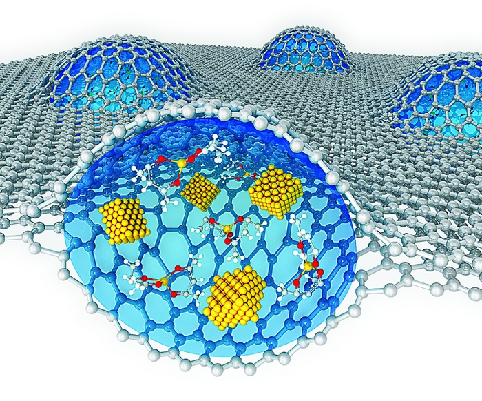
Chemical vapor method or CVD in the synthesis of crystal nanoparticles (PhD in nano-microelectronics)
Researcher and author: Dr. ( Afshin Rashid)
Note: Crystal nanoparticles are produced and amplified using various methods , such as CVD, laser irradiation and deburring . The CVD method is the best option for the industrial production of crystal nanoparticles. The reason for this is the low cost-to-income ratio as well as the possibility of vertical growth of crystal particles on the desired substrate .
In this process, the crystalline nanoparticles in the negative electrode are sublimated due to the high temperature in the discharge process. Since this method was first used for the synthesis of crystal nanoparticles , it is known as the most common method of producing crystal nanoparticles . In this method, which contains both types of crystal nanoparticles , single-walled and multi-walled, with lengths of up to 50 microns containing structural defects. In the laser irradiation process, the laser is used to evaporate the graphite and an inert gas is used to conduct these vapors into the tank. Crystal nanoparticles grow on the cold surface of the reactor . ایــن It is suitable for the production of crystal nanoparticles with multiple walls. And the use of composite graphite and metal catalyst particles combination of cobalt and nickel (for the synthesis of nano-crystals) is used. The efficiency of this process is 70 % and its main product is crystal nanoparticles . The diameter of these crystal nanoparticles is completely controllable and the diameter of the crystal nanoparticles can be controlled as desired by changing the temperature . CVD method with the help of catalysts for the production of nano-crystals used to be. During the CVD process, a layer of nickel, cobalt, and metal catalyst particles, usually iron, to produce Crystal nanoparticles are used . CVD is a common method for the commercial production of crystal nanoparticles . In this method, the diameter of the crystal nanoparticles is related to the dimensions of the metal particles. The diameter of the crystal nanoparticles can be controlled by sublayer patterning, heat treatment and pulsatile etching of the catalyst .
A crystal is made by arranging atoms and groups of atoms in regular patterns, for example at the corners of a cube or rectangle prism . The basic arrangement of the atoms that describes the crystal structure is determined. This cell is called a unit. The crystals must have a balanced charge . This means that the amount of negative charge must be compensated with the same amount of positive charge. A nanocrystal is a material particle having at least one dimension smaller than 100 nanometers, based on quantum dots . (A nanoparticle ) and consists of atoms arranged in either single or polycrystalline . The size of the nanocrystals distinguishes them from larger crystals .For example, silicon nanocrystals can emit efficient light, while bulk silicon does not and can be used for memory components. When embedded in solids, nanocrystals may exhibit much more complex melting behavior than conventional solids and may form the basis of a particular class of solids. They can act as single-domain systems (intra-system volumes with the same atomic or molecular arrangement) that can help explain the behavior of macroscopic specimens of the same material without the complexity and similarity of other particles . Semiconductor nano-crystals with dimensions less than 10 nm as well as quantum dots are described .Crystals whose refractive index is the same in all three crystal directions are called isotropic crystals. In contrast, crystals that have different refractive index in one, two or three directions are called anisotropic crystals. Nanoscale crystals, which are cut very frequently, are powerful catalysts for chemical reactions. And the unusual shape of the crystals causes the atoms of the nanocrystals to align themselves in an uneven way to increase reactivity.
Conclusion :
Crystal nanoparticles are produced and amplified using various methods , such as CVD, laser irradiation and deburring . The CVD method is the best option for the industrial production of crystal nanoparticles. The reason for this is the low cost-to-income ratio as well as the possibility of vertical growth of crystal particles on the desired substrate .
Researcher and author: Dr. ( Afshin Rashid)
PhD in Nano-Microelectronics


