

_ Department of nano- fullerence
Nanofluorescences and their application in various fields such as electronic applications (making nano electrodes used in certain electrical circuits, nano photonics in nano solar cells and nano absorbers of certain wavelengths)
Researcher and author: Dr. ( Afshin Rashid)
_z5nz.gif)
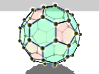
Note: Fullerenes are identified according to the number of atoms in their structure. A letter C is used to name fullerenes, which represents the carbon atom in their structure.
Fullerenes are among the materials that many nano materials are based on. Their unique structural and electronic properties, as well as their use in various fields such as electronic applications such as making nano electrodes used in special electrical circuits , nano photonics in nano solar cells and nano absorbers of specific wavelengths.
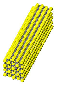
Layers of nanotubes can behave like a metal and be electrically angled. Changing the structure and building in them can show the characteristics of semiconductors. or be non-conductive . For example, a slight change in the helix can change the tube from a metal to a wide-gap semiconductor.
Layers of nanotubes can behave like a metal and be electrically angled. Changing the structure and building in them can show the characteristics of semiconductors. or be non-conductive . For example, a slight change in the helix can change the tube from a metal to a wide-gap semiconductor.

Conclusion :
The important feature of all nanostructures is that the number of surface atoms in them is more than the number of volume atoms. This ratio increases with decreasing nanoparticle size in fullerenes .
- Researcher and author: Dr. ( Afshin Rashid)
Specialized doctorate in nano-microelectronics