Nano Electro-Optical lithography Nano -lithography, What? (PhD in Nano _ Microelectronics)
Researcher and author: Dr. ( Afshin Rashid)
Note: Nano-lithography is a broad term used to describe various processes for creating nanoscale patterns in different environments, the most common of which is silicon semiconductor materials.
The predominant goal of nanolithography is to shrink electronic devices, which causes more electronic components to shrink into smaller spaces, that is, smaller integrated circuits that lead to smaller devices because they are faster and cheaper to produce because fewer materials are needed. It also increases performance and response time because electrons only have to travel very short distances.
Some of the techniques used in nanolithography are as follows:
_ Lito x-ray-using proximity printing runs and x-rays to the near field Fresnel diffraction is based. Its optical resolution has been increased to 15 nm.
Dual Patterning - A method used to increase the step resolution of a lithographic process by printing additional patterns between the spaces of previously printed patterns in a single layer.
Direct electron beam lithography (EBDW) - The most common process used in lithography that uses electron beam to create patterns.
Intense Ultraviolet Lithography (EUV) - A form of optical lithography that uses ultra-short wavelengths of light 13.5 nanometers.
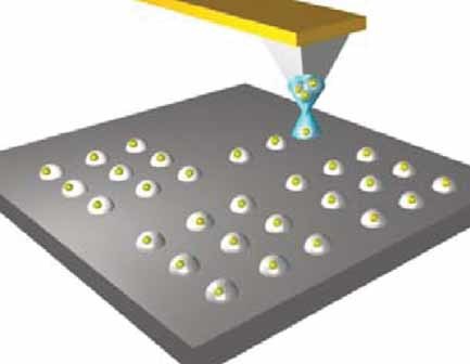
Nanolithography is a branch of nanotechnology and is the name given to the process of printing, writing, or engraving patterns on a microscopic surface to create ultra-small structures. This process is commonly used to create smaller and faster electronic devices such as micro / nanochips and processors. Nano-lithography is mainly used in various fields of technology from electronics to biomedicine. Nano-lithography is the art of creating structures at the nanometer scale. It may be used to create integrated circuits and components for semiconductor technology, where the ability to produce the smallest transistors and circuits may not only make it possible to create smaller devices, but can also help increase the efficiency and performance of components.Advances in lithographic methods have also made it possible to construct complex structures that can be used for microelectromechanical or nanoelectromechanical devices (MEMS or NEMS). Such miniature machines have previously been used as pH sensors and transistors, but there are many future advances in such technologies as the use of devices for drug delivery.
Conclusion :
Nano-lithography is a broad term used to describe various processes for creating nanoscale patterns in different environments, the most common of which is silicon semiconductor materials.
Researcher and author: Dr. ( Afshin Rashid)
PhD in Nano-Microelectronics


