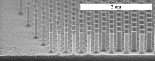
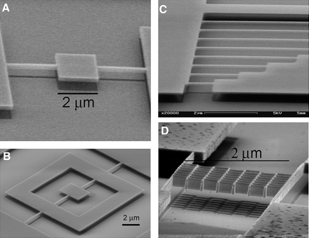
Scanning Probe Nano Lithography (SPL) Using Atomic Force Microscope (AFM) in the manufacture of nanoelectronic devices and tools (PhD in Nano-Microelectronics)
Researcher and author: Dr. ( Afshin Rashid)
Note: The tip of a scanning tunneling microscope (STM) or atomic force microscope (AFM) offers not only imaging capabilities up to atomic resolution, but also nanostructured capabilities with such excellent resolution. An example is the paradigm of building a furnace by manipulating individual atoms on the surface using nano-lithography scanning probes .
Although the speed of making such a thing has recently improved , it is a process with major problems in scaling and integrating with the semiconductor industry. Using an atomic force microscope to scan the lithography probe The nano-lithography probe of the scanning probe also suffers from power problems, but due to the less stringent requirements of this technique, it is more suitable than a scanning tunneling microscope: without ultra-high vacuum conditions. , A very conductive surface or a very good control of the distance between the tip to the sample is required. Scanning probe nano-lithography based on scanning tunneling microscopy can be performed through various mechanisms and offers a wide range of possibilities. Thus, the tip of an atomic force microscope can make local changes in the composition, height, or physical / chemical properties of surfaces through thermal effects, mechanical effects, deposition, chemical effects, and so on. In fact, a very popular derivative technique is dip-pen nano-lithography, in which the tip of certain inks is placed with great resolution in the desired locations.
Scanning probe nano-lithography , respectively, uses a concentrated ion or an electron beam to separate a precursor gas. Nano-lithography techniques are direct additives that allow specific materials to grow in desired locations without the need for resistance. . They can be used in contexts in which processing of resistance, like the tip of the cantilever are not suitable, use the purity of the materials stored by nano-lithography, scanning probe can be an issue and the methods of treatment during or after growth for growth of three Next with very high lateral resolution are suitable. As a sequential technique, scanning probe nano-lithography is inherently slow and not suitable for large nanoparticles. Recent developments using cryogenic temperatures to compress the precursor, the growth rate increases several times, this technique called nano-lithography, scanning probe known Shvnd.bh general applications of nano-lithography, scanning probe generally Circuit editing and mask repair in the semiconductor industry and the protection of cross-sectional imaging and preparation and prototyping, as well as the construction of nanostructures in the fields of nanotechnology are related.
Conclusion :
The tip of a scanning tunneling microscope (STM) or atomic force microscope (AFM) offers not only imaging capabilities up to atomic resolution, but also nanostructured capabilities with such excellent resolution. An example is the paradigm of building a furnace by manipulating individual atoms on the surface using nano-lithography scanning probes .
Researcher and author: Dr. ( Afshin Rashid)
PhD in Nano-Microelectronics


