

_ Department of nanoelectronics and (plasmonic waves)
Investigating the structure of nanoelectronics and (plasmonic waves) electromagnetic waves and conduction electrons
Researcher and author: Dr. ( Afshin Rashid)
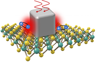
Note: These nanostructures consist of metal and dielectric, whose dimensions are below the excitation wavelength (the wavelength of the radiation that causes the excitation of plasmonic waves).
Further compression of the structure of electronic devices and accessories with the help of plasmonic science , caused the use of plasmonic structures and plasmonic waves to be investigated and used. Plasmonic is based on the process of interaction between electromagnetic waves and conduction electrons in metals with nano dimensions. Analytically, the reason is the rapid drop in the energy of electrons passing through metals, and it was concluded that this energy is spent on the cumulative movement and oscillation of the free electrons of the metal and called it plasmon. With the approach of technology towards the accumulation of opto-electronic circuits, manufacturing problems and phenomena that helped prevent further compression of the structure, caused the use of plasmonic structures and plasmonic waves to be investigated and used. These nanostructures consist of metal and dielectric, whose dimensions are below the excitation wavelength (the wavelength of the radiation that causes the excitation of plasmonic waves).


In electronic science, the topic of nano revolves around (nano memories, nano chips and fast nano chips and nano electronic components) with less weight and more efficiency. Nanotechnology, knowledge, engineering and technology on a nano scale, or in other words, studying the application of very small objects and their use in all fields of science such as chemistry, biology, electronics; Material science and engineering. The history of nanotechnology describes the development of concepts and experimental work done in the field of nanotechnology. Although nanotechnology is one of the recent advances in scientific research, the development of its fundamental concepts has taken place over a long period of time. All kinds of nano technologies, such as more compression of the structure of electronic devices and accessories , etc., cannot cope with all the practical demands of industrial applications in terms of high resolution, high power, and low cost. , large area and patterns on non-flat and curved surface. Therefore, new high-volume nano-manufacturing technology urgently needs to be exploited and developed to meet the extraordinary needs of growing markets.

Conclusion :
Further compression of the structure of electronic devices and accessories with the help of plasmonic science , caused the use of plasmonic structures and plasmonic waves to be investigated and used. These nanostructures consist of metal and dielectric, whose dimensions are below the excitation wavelength (the wavelength of the radiation that causes the excitation of plasmonic waves).
Researcher and author: Dr. ( Afshin Rashid)
Specialized doctorate in nano-microelectronics