

_ Department of nanoelectronics and (plasmonic waves)
Investigation of small changes in the dielectric around the nano volume on the resonance of surface plasmons
Researcher and author: Dr. ( Afshin Rashid)
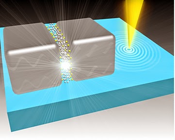
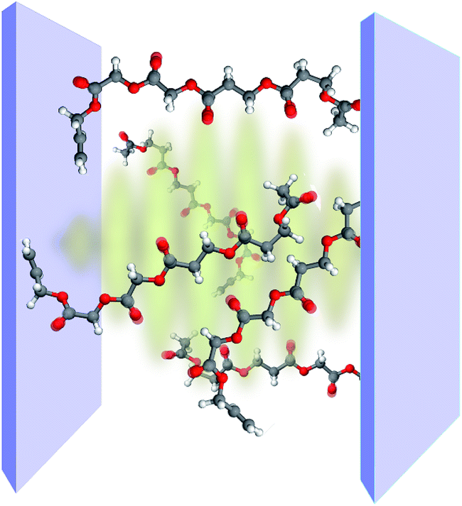
Note: Small changes in the dielectric around the nano volume affect the resonance of surface plasmons, so that these changes show themselves in the amount of scattered light, absorbed light or change in its wavelength.
In the building of nanostructures (nanoplasmonics), the created volume of the electromagnetic field is localized, compressed and improved. Nanostructure is defined as any structure with one or more dimensions and is measured in the range of nanometer scale. Nanostructures refer to materials or structures that have at least one dimension between 1 and 100 nanometers . The importance of nanoscale is in changing the properties and characteristics of materials in these dimensions. Properties such as electrical conductivity, electromagnetic properties, etc. Starting to change the properties of the material by shrinking it depends above all on the type of material and the desired property. For example, by shrinking the dimensions of a material, generally some of the electromagnetic properties of nano-molecular materials such as the conductivity of nano particles in materials are improved. This increase in strength does not happen only in the range of a few nanometers, and the strength of materials of several tens or even hundreds of nanometers may be much higher than the mass material of a large scale. These changes can be measured using optical characteristics. It shows the oscillation of surface electrons and the electric field around them in the resonance of localized surface plasmons.
For example, by reducing the dimensions of a nanostructure material (nanoplasmonics) , generally some mechanical properties of the material such as strength are improved. This increase in strength does not happen only in the range of a few nanometers, and the strength of materials of several tens or even hundreds of nanometers may be much higher than large-scale mass materials. On the other hand, the change of some properties such as color and magnetic properties may occur in dimensions of only a few nanometers. Nano plasmonics is expressed based on the process of interaction between electromagnetic waves and conduction electrons in metals with nano dimensions , analytically it is the reason for the rapid energy loss of electrons passing through metals and it was concluded that this energy is spent on cumulative movement and species oscillation Free electrons become metal and it is called plasmon. These nanostructures consist of metal and dielectric, whose dimensions are below the excitation wavelength (the wavelength of the radiation that causes the excitation of plasmonic waves).

Conclusion :
In the building of nanostructures (nanoplasmonics), the created volume of the electromagnetic field is localized, compressed and improved. Small changes in the dielectric around the nano volume affect the resonance of surface plasmons, so that these changes show themselves in the amount of scattered light, absorbed light or change in its wavelength.
Researcher and author: Dr. ( Afshin Rashid)
Specialized doctorate in nano-microelectronics