

Nanoelectro Systems ( NEMS ) The integration of nanoelectric elements, sensors, actuators, and nanoelectronic devices on a silicon basis by micron-sized manufacturing technology (PhD in Nano-Microelectronics)
Researcher and author: Dr. ( Afshin Rashid)
Note: Recent trends in nanoelectronics engineering and science have focused on emphasizing the combination, analysis, and control of advanced MEMS and NEMS . The processes of composition, design , and optimization are in fact evolutionary over natural samples .
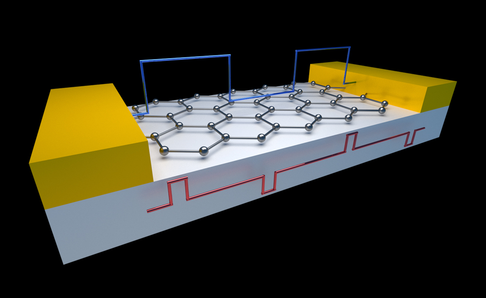
At each level of the design hierarchy, the efficiency of the system in the realm of its behavior is used to evaluate, optimize, and correct the optimization and composition process to find new solutions. ICs must meet the performance characteristics of MEMS, such as electromagnetic-based electromechanical devices and structures , input-output channels, analog-to-digital conversions, and analog-to-analog data. Micro-electro-mechanical systems (MEMS, (complex of mechanical elements, sensors, actuators and components electronic silicone-based technology by building about the size of microns. As long as the devices for electronic circuits for use in processIntegrated ICs (such as component processes ), "BICMOS, Bipolar, CMOS micromechanical fabrication " for use in micro- machining processes, suitable for selectively adding layer by layer with silica tablets new building for shaping devices mechanical and electromechanical used, are made. MEMS promises to revolutionize modern in the field of integrated silicon-based technology, microelectronics and micro are not, that in order to make possible the full realization of "systems In a "chip".

MEMS is a technology that allows the development of intelligent products , complementing the computing power of microelectrons, taking into account the capabilities of microsensors and micromotors, and the development of possible design and use space. Microelectronic integrated circuits can be considered as the mastermind of a system, and MEMS has enhanced this decision-making capability with eyes and arms to allow microsystems to measure the environment by mechanical, temperature, biological, chemical, They collect light and magnetism. The electronics then display information taken from the sensors and through some decisions to the arms to react by moving, stabilizing the position, Commands setting, pumping and filtering . As a result, the environment is controlled for the desired demands . Because MEMS devices are built for use in group manufacturing methods such as integrated circuits , new levels of performance, reliability, and skill can be achieved on a small silicon chip at a relatively low cost and low MEMS availability. Different specifications should be designed according to the needs, purposes and applications: MEMS and NEMS Electromechanical or mechanical electronics have been developed.
Usually "system of optical faster, easier and more efficient, more reliable and more durable than electromechanical systems are. If what optical systems for various applications are designed (such as communications, computing and switching, wireless, etc.), configurations different in general, it is very difficult that a comparative study between them do. for example, the optical system can not be used as stimuli to be applied. requirements Applications must be counted and fittings, electromagnetic, temperature, vibration or radiation The factors used to build can be better: the size of the actuator to the mass of force or torque that is a function of the material Used and its size (volume) depends. In fact, the size is determined by the required force and torque and its gender . The fact that electromagnetic MEMS, microstructures or Micro Trans Dyvsdhayy with IC used in Myykrv radiant energy devices are controlled, are complex, very important is. Thus, microstructures and microstransmitters , radiant energy devices, and ICs must be integrated. Direct chip connection technology has advanced extensively. In particular, the chip-flip MEMS suite was replaced with wired tape to connect the ICs to the micro-nanostroke actuators and sensors. Using chip-flip technology, the possibility of removing inductors and Provides capacitors and noise resistance. This leads to the modification of the device specifications. Continuing chip-flip integration leads to the benefits of implementing advanced flexible packages , reliable improvements and weight and size reductions, and so on . Integrated chip-flip, diode microtransformers can be mounted with protrusions and downwards on layers mounted on electromechanical devices and attached to the IC base. MEMS Large-scale integrated MEMS (a chip that can be mass-produced) And at a low cost used in COMS,

Conclusion :
Recent trends in nanoelectronics engineering and science have focused on emphasizing the combination, analysis, and control of advanced MEMS and NEMS . The processes of composition, design , and optimization are in fact evolutionary over natural samples .
Researcher and author: Dr. ( Afshin Rashid)
PhD in Nano-Microelectronics