

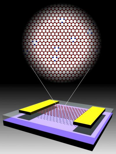
Section "Nanospin Electrons" - Nanoelectronics
A final and general summary of the topic of nano (spintronics) and "nano spin electrons" __ a final impression of this topic
Researcher and author: Dr. ( Afshin Rashid)
Note: Most of the devices that are used today in the nano-microelectronics industry use electron charge to communicate and store information, and it is mostly used in the manufacture of nanochips and nanoswitches.
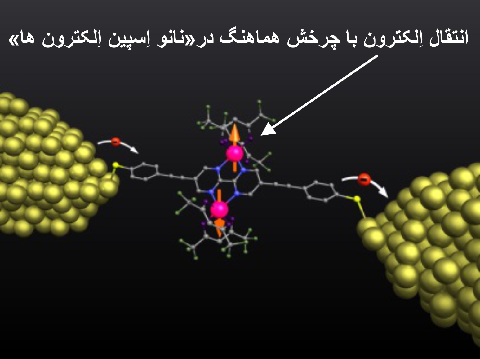
In nanospintronics technology, spin or the intrinsic angular momentum of the electron is considered to be the way to use this factor for two important discoveries based on this technology. First, resistance tunneling phenomenon was predicted. Based on this phenomenon, the degree of electron tunneling from an insulating layer can be called magnetization by placing two ferromagnetic layers on both sides of it and manipulating the relative direction of magnetization of these two. But this phenomenon alone controlled the ability of the layer.
This nanospin structure and magnetic tunnel connection were not used in the industry; To change the magnetization of the ferromagnetic layer, an external magnetic field had to be used, which caused many problems. In this case, it is possible to change the magnetization using 1-spin current, practically enabling the use of the magnetic resistance tunneling phenomenon. It is said that the method to change the magnetization of the spin torque transfer can be made a variable resistance using this technology. Variable resistance can be used both for data storage and for switching. The working mechanism of this technology is defined to change the resistance.
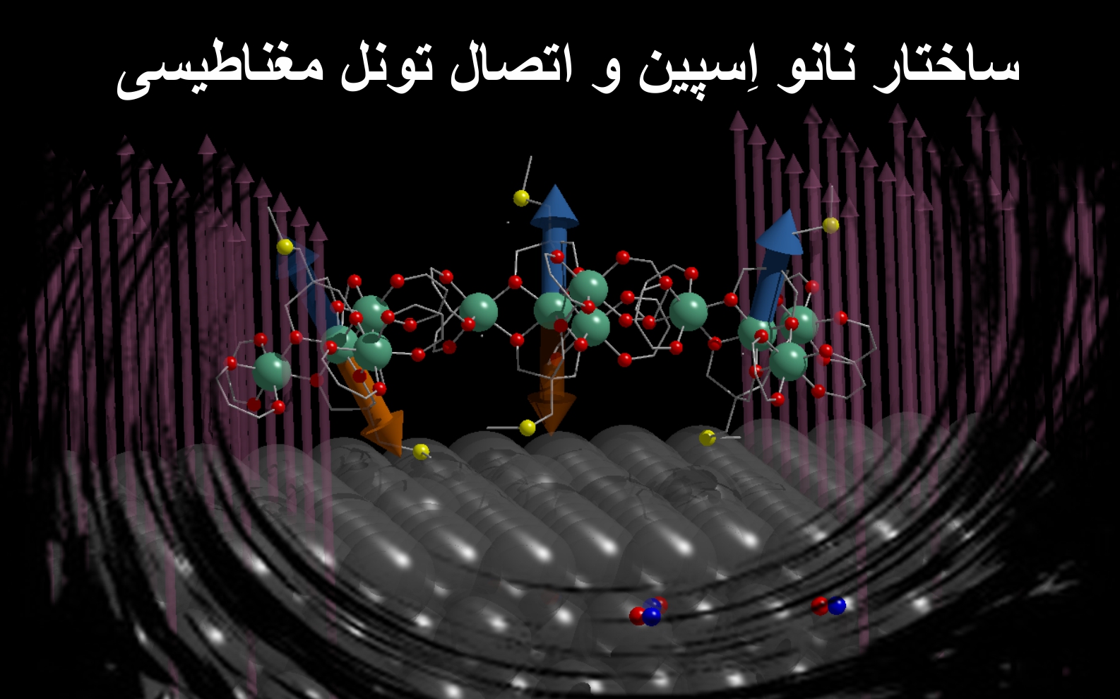
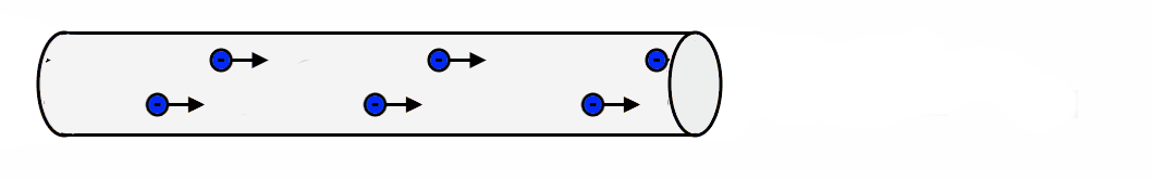
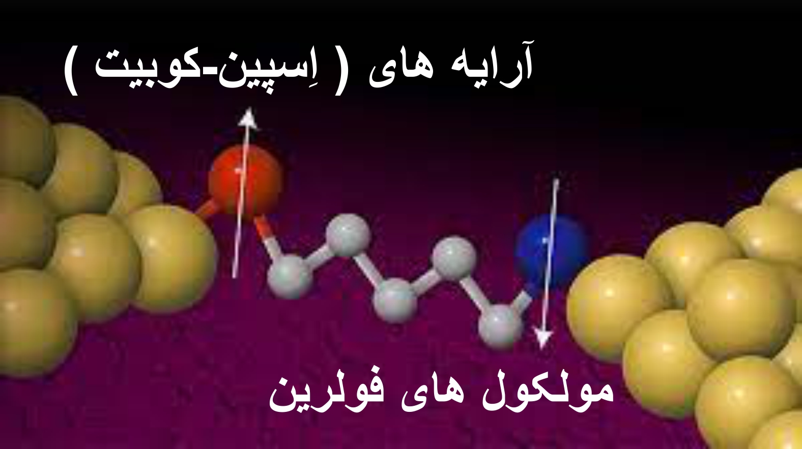
Nano-electrons of opposite spin and tunneling between electronic nano-layers
When the current enters the connection from the side of the lower layer whose magnetism is constant and unchanged, those electrons, which have spin in the direction of the magnetism of this layer, can tunnel and enter the upper ferromagnetic layer. As a result, the magnetism of the upper layer will be aligned with the lower layer and this will reduce the resistance in this connection. But if the current enters the connection from the upper layer that has the possibility of changing the magnetization, the electrons that have the opposite spin to the direction of the magnetization of the lower layer will be reflected and will not be able to tunnel. As a result, the magnetism of the upper layer goes against the direction of the lower layer and the connection resistance increases.

Conclusion :
Researcher and author: Dr. ( Afshin Rashid)
Specialized doctorate in nano-microelectronics