

_Part of endohedral nanostructures
( endohedral nanostructures) in nano-optical devices (xAs-AlxGa1) in (x<45.0 mode)
Researcher and author: Dr. ( Afshin Rashid)
Note: ( endohedral nanostructures) in nano-optical devices (xAs-AlxGa1) is found in (x<45.0 mode) along with changes in the distance between the edge of the valence band and the edge of the conduction band with the change of x in three different directions of wave propagation.
Due to the lack of suitable insulation for use in gate transistors, as well as the high cost of elements and the layering process of compound semiconductors, silicon and finally silicon-germanium alloy are still used as the main semiconductor. It should be mentioned ( endohedral nanostructures) , which can be easily layered with high purity, is a very suitable insulator for this purpose. Nowadays, in integrated circuits with channel length below 50 nm, substitute oxides with higher dielectric coefficient such as zirconium oxide, ZrO2 and hafnium oxide are used. reached For example, in xAs-AlxGa1 and xN-InxGa1, the change of x leads to the change of energy gap and many properties of these compound semiconductor materials lead to the energy of the band structure.
_y6zn.gif)
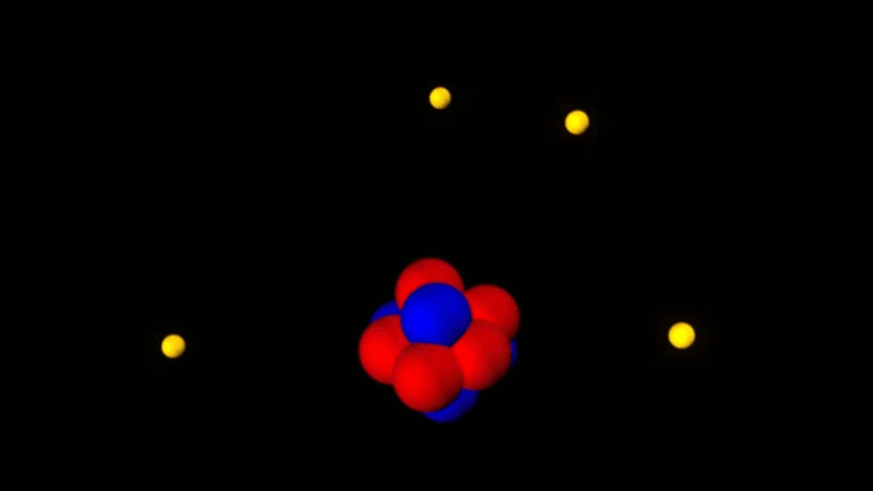
One of the most important properties ( endohedral nanostructures) is the electronic property. (endohedral nanostructures) is a semiconductor with zero band gap and high electrical conductivity . As we know, each carbon atom has 1 electron that participates in chemical bonds, but in graphene, each carbon atom is connected to 9 other carbon atoms in a two-dimensional space. The remaining single atoms create pie orbitals at the top and bottom of the graphene sheet and these orbitals create carbon-carbon double bonds. Electronic properties are imposed on graphene by (bonding orbitals) and ( antibonding) double bonds. Graphene shows very high electron mobility at ambient temperature.
The optical strength of metal nanoparticles is 22, the breaking strength is 12 mN, and its Young's coefficient is Tpa 4. Despite its high hardness and strength, it is very light and its density is 1.77 ml/mg. The (optical) properties of the monolayer membrane of metal nanoparticles are measured by AFM technique.

Conclusion :
( endohedral nanostructures) in nano-optical devices (xAs-AlxGa1) in (x<45.0 mode) along with changes in the distance between the edge of the valence band and the edge of the conduction band with the change of x in three different directions of wave propagation.
Researcher and author: Dr. ( Afshin Rashid)
Specialized doctorate in nano-microelectronics